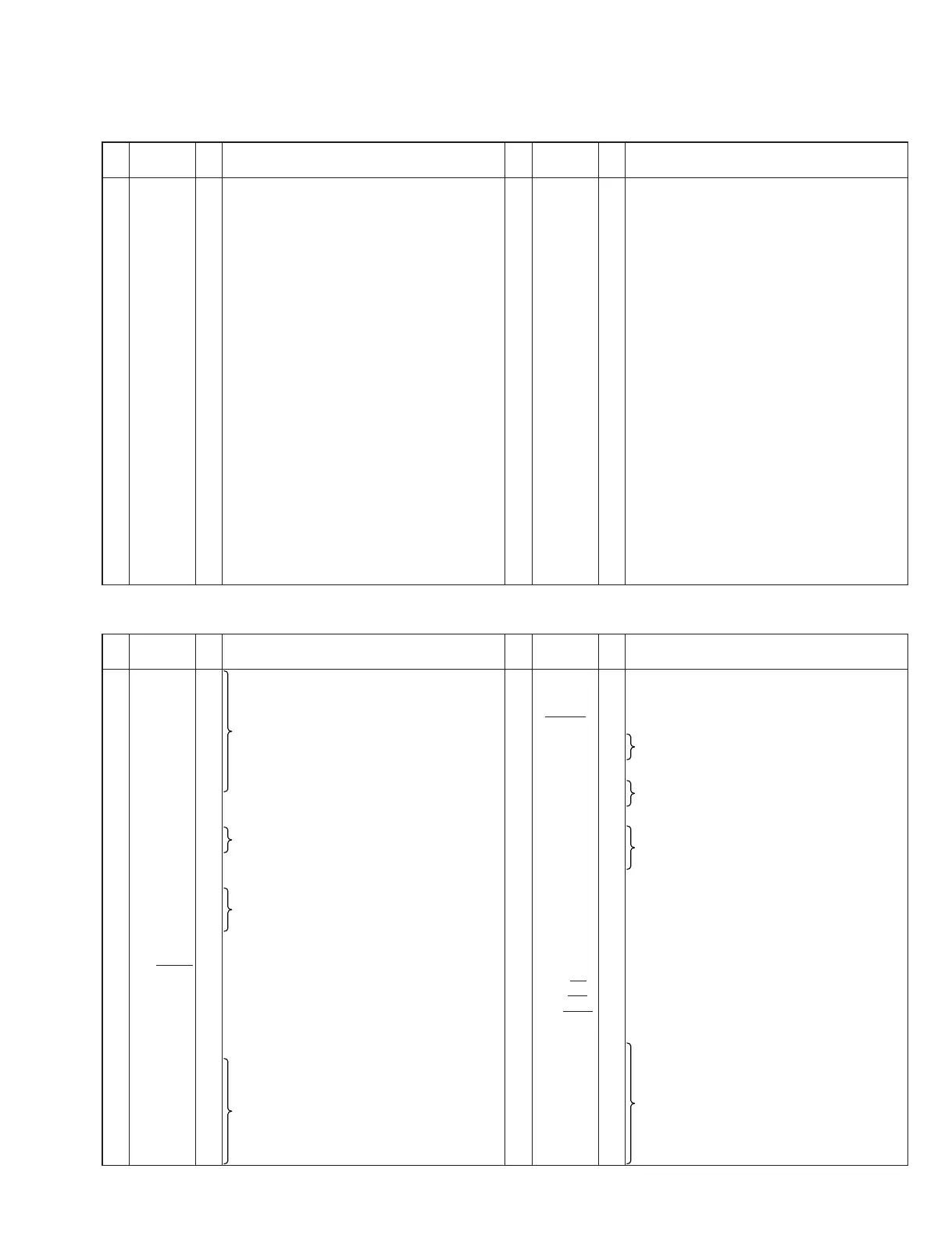
PIN
NO.
NAME I/O FUNCTION
33 P10/ANI0 I Port 1 / A/D converter analog input
34 AVREF I A/D converter reference voltage input
35 AVDD – Analog power supply +5 V
36 RESET I System reset input
37 XT2 –
Subsystem clock oscillation
38 XT1 I
39 IC – Internally connected
40 X2 –
Main system clock oscillation
41 X1 I
42 Vss1 – Ground
43 P00/INTP0 I/O
44 P01/INTP1 I/O Port 0 / External interrupt request input
45 P02/INTP2 I/O
46
P03/INTP3/ADTRG
I/O
Port 0 / External interrupt request input / Trigger signai input
47
P70/TI00/TO0
I/O
Port 7 / External count clock input / 16-bit timer/event counter 0 output
48 P71/TI01 I/O Port 7 / Capture trigger input
49
P72/TI50/TO50
I/O
Port 7 / External count clock input / 8-bit timer/event counter 50 output
50
P73/TI51/TO51
I/O
Port 7 / External count clock input / 8-bit timer/event counter 51 output
51 P74/PCL I/O Port 7 / Clock output
52 P75/BUZ I/O Port 7 / Buzzer output
53 P64/RD I/O Port 6 / Strobe signal output for reading
54 P65/WR I/O Port 6 / Strobe signal output for writing
55 P66/WAIT I/O Port 6 / Wait insertion
56 P67/ASTB I/O Port 6 / Strobe output
57 P40/AD0 I/O
58 P41/AD1 I/O
59 P42/AD2 I/O
60 P43/AD3 I/O
Port 4 / Lower address/data bus
61 P44/AD4 I/O
62 P45/AD5 I/O
63 P46/AD6 I/O
64 A47/AD7 I/O
PIN
NO.
NAME I/O FUNCTION
1 P50/A8 I/O
2 P51/A9 I/O
3 P51/A10 I/O
4 P53/A11 I/O
Port 5 / Higher address bus
5 P54/A12 I/O
6 P55/A13 I/O
7 P56/A14 I/O
8 P57/A15 I/O
9 Vss0 – Ground
10 V
DD
0 – Power supply +5 V
11 P30 I/O
Port 3
12 P31 I/O
13 P32/SDA0 I/O Port 3 / Serial data input/output
14 P33/SCL0 I/O Port 3 / Serial clock input/output
15 P34 I/O
16 P35 I/O Port 3
17 P36 I/O
18 P20/SI30 I/O Port 2 / Serial data input
19 P21/SO30 I/O Port 2 / Serial data output
20
P22/SCK30
I/O Port 2 / Serial clock input/output
21 P23/RxD0 I/O Port 2 / Serial data input
22 P24/TxD0 I/O Port 2 / Serial data output
23
P25/ASCK0
I/O Port 2 / Serial clock input/output
24 V
DD
1 – Power supply +5 V
25 AVss – Ground
26 P17/ANI7 I
27 P16/ANI6 I
28 P15/ANI5 I
29 P14/ANI4 I Port 1 / A/D converter analog input
30 P13/ANI3 I
31 P12/ANI2 I
32 P11/ANI1 I
PIN
NO.
NAME I/O FUNCTION
23 P42 I/O Port 42
24 P43 I/O Port 43
25 P44 I/O Port 44
26 P45 I/O Port 45
27 P46 I/O Port 46
28 P47 I/O Port 47
29 P74 I/O Port 74
30 P75 I/O Port 75
31 P76 I/O Port 76
32 P77 I/O Port 77
33 P90 I/O Port 90
34 P91 I/O Port 91
35 P80 I/O Port 80
36 P81 I/O Port 81
37 P70 I/O Port 70
38 P71 I/O Port 71
39 P72 I/O Port 72
40 P73 I/O Port 73
41 PB4 I/O Port B4
42 PB5 I/O Port B5
43 PB6 I/O Port B6
44 PB7 I/O Port B7
•
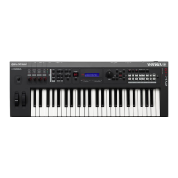
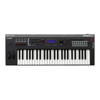
TMP89FM42AUG (YC778D00) MICROCONTROLLER
DM: IC402
•
μPD780031AYGK-N09-9ET-A (XZ916300) LED/SWITCH DRIVER
PNA: IC601
PIN
NO.
NAME I/O FUNCTION
1 VSS – Ground
2 XIN I
High frequency departure pendulum connection terminal
3 XOUT O
High frequency departure pendulum connection terminal
4 MODE I
Terminal for shipment examination / Please fix at “L” level
5 VDD – Power supply +5D
6 P02 I/O Port 02
7 P03 I/O Port 03
8 /RESET I System reset input
9 P11 I/O Port 11
10 P12 I/O Port 12
11 P13 I/O Port 13
12 P20 I/O Port 20
13 P21 I/O Port 21
14 P22 I/O Port 22 / Serial clock I/O 0
15 SDA0 I/O Serial bus data input/output
16 SCL0 I/O Serial bus data input/output
17 P25 I/O Port 25
18 P26 I/O Port 16
19 P27 I/O Port 27
20 VAREF/
Analog, standard voltage input terminal for analog to
AVDD
digital translation / Power supply terminal for analogue
21 AIN0 I A/D converter analog input
22 P41 I/O Port 41
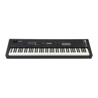
17
MX61/MX49