■
LSI PIN DESCRIPTION
(LSI 端子機能表)
CONTENTS
(目次)
• AK4385ET (X6040A01) DAC (Digital to Analog Converter) .................................................................... 14
• R8A02042BG (YC479A00) SWX08 ........................................................................................................ 15
• TAS1020BPFBR (YA413A00) USB CONTROLLER ............................................................................... 14
• TMP89FM42AUG (YC778D00) MICROCONTROLLER ......................................................................... 17
• μPD780031AYGK-N09-9ET-A (XZ916300) LED/SWITCH DRIVER ......................................................17
•
AK4385ET (X6040A01) DAC (Digital to Analog Converter)
DM: IC310
•
TAS1020BPFBR (YA413A00) USB CONTROLLER
DM: IC304
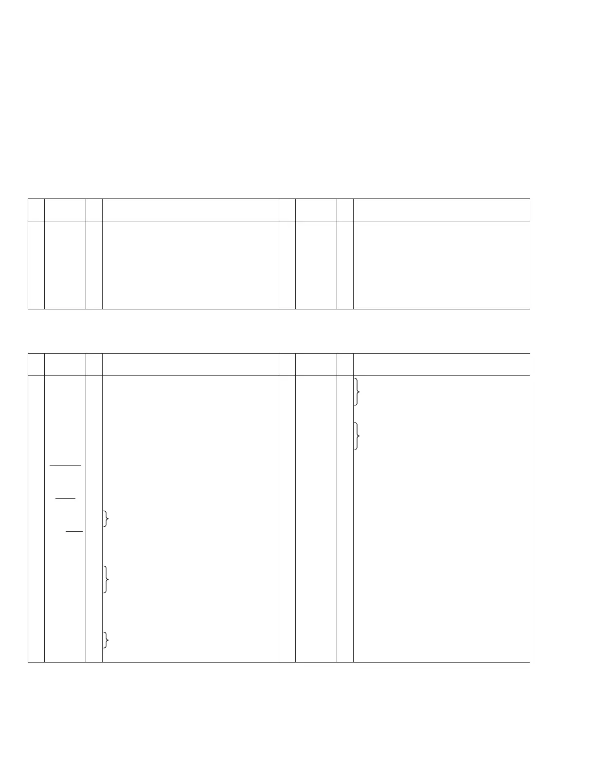
PIN
NO.
NAME I/O FUNCTION
1 MCLK I Master Clock
2 BICK I Audio Serial Data Clock
3 SDTI I Audio Serial Date Input
4 LRCK I L/R Clock
5 PDN I Power Down mode
6 CSN I Chip Select
7 CCLK I Control Data Input
8 CDTI I Control Data Input
PIN
NO.
NAME I/O FUNCTION
9 AOUTR- O Rch Analog out(-)
10 AOUTR+ O Rch Analog out(+)
11 AOUTL- O Lch Analog out(-)
12 AOUTL+ O Lch Analog out(+)
13 Vss – Ground
14 VDD – Power Supply
15 DZFR O Rch Data Zero Input Detect
16 DZFL O Lch Data Zero Input Detect
PIN
NO.
NAME I/O FUNCTION
1 PLLFILO O PLL loop filter output
2AV
DD
– +3.3V analog supply voltage
3 MCLKI I Master clock input
4 DVss – Digital ground
5 PUR – USB data signal plus pullup resistor connect
6 DP I/O USB differential pair data signal plus
7 DM I/O USB differential pair data signal minus
8DV
DD
– +3.3V digital supply voltage
9 MRESET I Master reset
10 TEST I Test mode enable
11 EXTEN I External MCU mode enable
12 RSTO O Reset output
13 P3.0 –
General-purpose I/O port [bits 0 through 1]
14 P3.1 I/O
15 P3.2/XINT I/O General-purpose I/O port [bits 0 through 1] /
External interrupt
16 DVss – Digital ground
17 P3.3 I/O
18 P3.4 I/O General-purpose I/O port [bits 0 through 1]
19 P3.5 I/O
20 NC – Not used
21 DV
DD
– +3.3V digital supply voltage
22 NC – Not used
23 P1.0 I/O
General-purpose I/O port [bits 0 through 1]
24 P1.1 I/O
PIN
NO.
NAME I/O FUNCTION
25 P1.2 I/O
26 P1.3 I/O General-purpose I/O port [bits 0 through 1]
27 P1.4 I/O
28 DVss – Digital ground
29 P1.5 I/O
30 P1.6 I/O General-purpose I/O port [bits 0 through 1]
31 P1.7 I/O
32 CSCHNE I/O Codec port interface secondary channel enable
33 DV
DD
– +3.3V digital supply voltage
34 CRESET I/O Codec port interface reset output
35 CSYNC I/O Codec port interface frame sync
36 CDATI I/O Codec port interface serial data in
37 CSCLK I/O Codec port interface serial clock
38 CDATO I/O Codec port interface serial data out
39 MCLKO1 O Master clock output 1
40 MCLKO2 O Master clock output 2
41 RESET O General-purpose active-low output
which is memory mapped
42 VREN O General-purpose active-low output
which is memory mapped
43 SDA I/O I2C interface serial data
44 SCL O I2C interface serial clock
45 AVss – Analog ground
46 XTALO O Crystal Output
47 XTALI I Crystal input
48 PLLFILI I PLL loop filter input
14
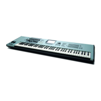
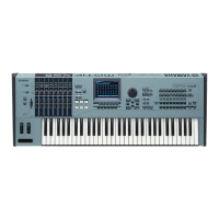
MX61/MX49