Do you have a question about the Yamaha SPX1000 and is the answer not in the manual?
Detailed electrical characteristics including frequency response, dynamic range, distortion.
Specifications for input channels, level, and impedance.
Specifications for Analog-to-Digital conversion, sampling frequency, and quantization.
Specifications for Digital-to-Analog conversion, sampling frequency, and quantization.
Specifications for output channels, level, and impedance.
Details on presets (ROM) and user memory (RAM) capacity.
Specifications for MIDI control messages like Program Change and Control Change.
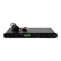
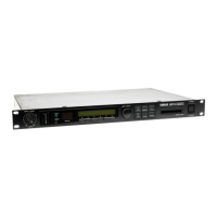
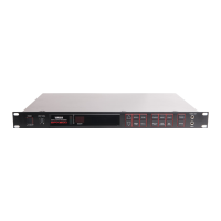
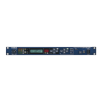
Details about front panel controls, keys, and display.
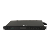
List of connectors and their functions on the front and rear panels.
Details about rear panel connectors and switches.
List of switches and their functions.
General specifications including power supply and dimensions.
Circuit board layout and wiring diagram for US and Canadian models.
Circuit board layout and wiring diagram for the European model.
Circuit board layout and wiring diagram for the Japanese model.
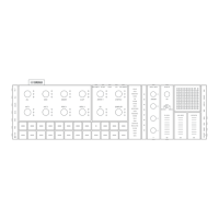
Detailed layout and identification of controls on the front panel.
Detailed layout and identification of connectors and controls on the rear panel.
Instructions for removing the top cover of the unit.
Instructions for removing the front panel of the unit.
Instructions for removing the AD circuit board.
Instructions for removing the PS circuit board.
Instructions for removing the MT circuit board.
Instructions for removing the FP 1/3 circuit board.
Instructions for removing the FP 2/3 circuit board.
Instructions for removing the FP 3/3 circuit board.
Instructions for removing the LCD assembly.
Initial setup and connections required for checks and adjustments.
Procedures for adjusting various parameters like clipping level, gain, MSB, and offset.
Procedure for adjusting output gain levels based on switch settings.
Procedure for measuring and verifying frequency response.
Procedure for measuring and verifying distortion levels.
Procedure for measuring and verifying noise levels.
Procedure for measuring maximum output level and distortion.
Procedure for measuring channel separation and signal leakage.
Procedure for checking the muting circuit operation during power on/off.
Specifications for measuring instruments used in checks and adjustments.
Conditions for transmitting MIDI data, including channel and bulk data.
Detailed structure and format of transmitted MIDI data, including system information.
Specifics of system information transmission via MIDI, including memory bulk data.
Format for transmitting bank program change chart data via MIDI.
Format for transmitting user ER pattern data via MIDI.
Format for transmitting system setup data via MIDI.
Conditions for receiving MIDI data, including channel and trigger settings.
Details on received MIDI data, including channel voice messages and system exclusive messages.
Interpretation of channel voice messages like Note On and Note Off.
Interpretation of system exclusive messages like bulk dump requests.
How control change messages are received and used to control parameters.
How program change messages are received to load programs.
Format for Bank Change Request MIDI messages to switch banks.
Diagram illustrating analog input/output signal flow.
Diagram illustrating 'Pre' digital I/O mode signal flow.
Diagram illustrating 'Post' digital I/O mode signal flow.
Diagram illustrating digital input/output signal flow.
Description of single effect modes from #1 to #30.
Description of multi-effect modes from #31 to #33.
Description of 2-channel in effect modes from #34 to #38.
Description of stereo effect modes #39 and #40.
Instructions on how to enter and start the test program.
Procedure for testing the LCD display functionality.
Procedure for testing all LED indicators and segments.
Procedure for checking all panel switches using foot switches.
Procedure for checking the FOOT VOLUME 1 control.
Procedure for checking the FOOT VOLUME 2 control.
Procedure for checking the analog trigger input (LINE).
Procedure for checking the analog trigger input (MIC).
Procedure for checking MIDI IN/OUT communication.
Procedure for adjusting AD offset and minimizing click noise.
Procedure for initializing the unit to factory settings.
Procedure for checking the DRAM for DSP.
Component layout diagram for the AD circuit board.
Component layout diagram for the FP 1/3 circuit board.
Component layout diagram for the FP 2/3 circuit board.
Component layout diagram for the FP 3/3 circuit board.
Component layout diagram for the MT circuit board.
Component layout diagram for the Japanese PS circuit board.
Component layout diagram for the U.S. PS circuit board.
Component layout diagram for the Canadian PS circuit board.
Component layout diagram for the North European PS circuit board.
| Sampling Frequency | 44.1 kHz |
|---|---|
| Dynamic Range | 90 dB |
| Type | Multi-Effect Processor |
| Frequency Response | 20 Hz - 20 kHz |
| MIDI | In, Out |
| Memory | 7 user programs |
| Total Harmonic Distortion + Noise | 0.03% (1 kHz) |
| Effects Programs | 63 programs |
| Effects Types | Reverb, Delay, Modulation, Pitch, EQ |
| Power Supply | AC 120V |
| Dimensions (W x D x H) | 480 mm |