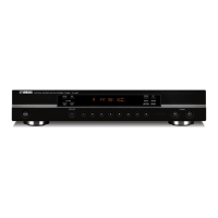
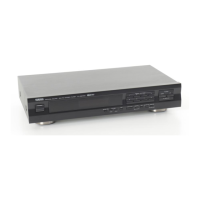
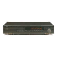
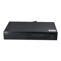
TX-497
A
1
2
3
4
5
6
7
8
9
BCDEFGH I JKL
22
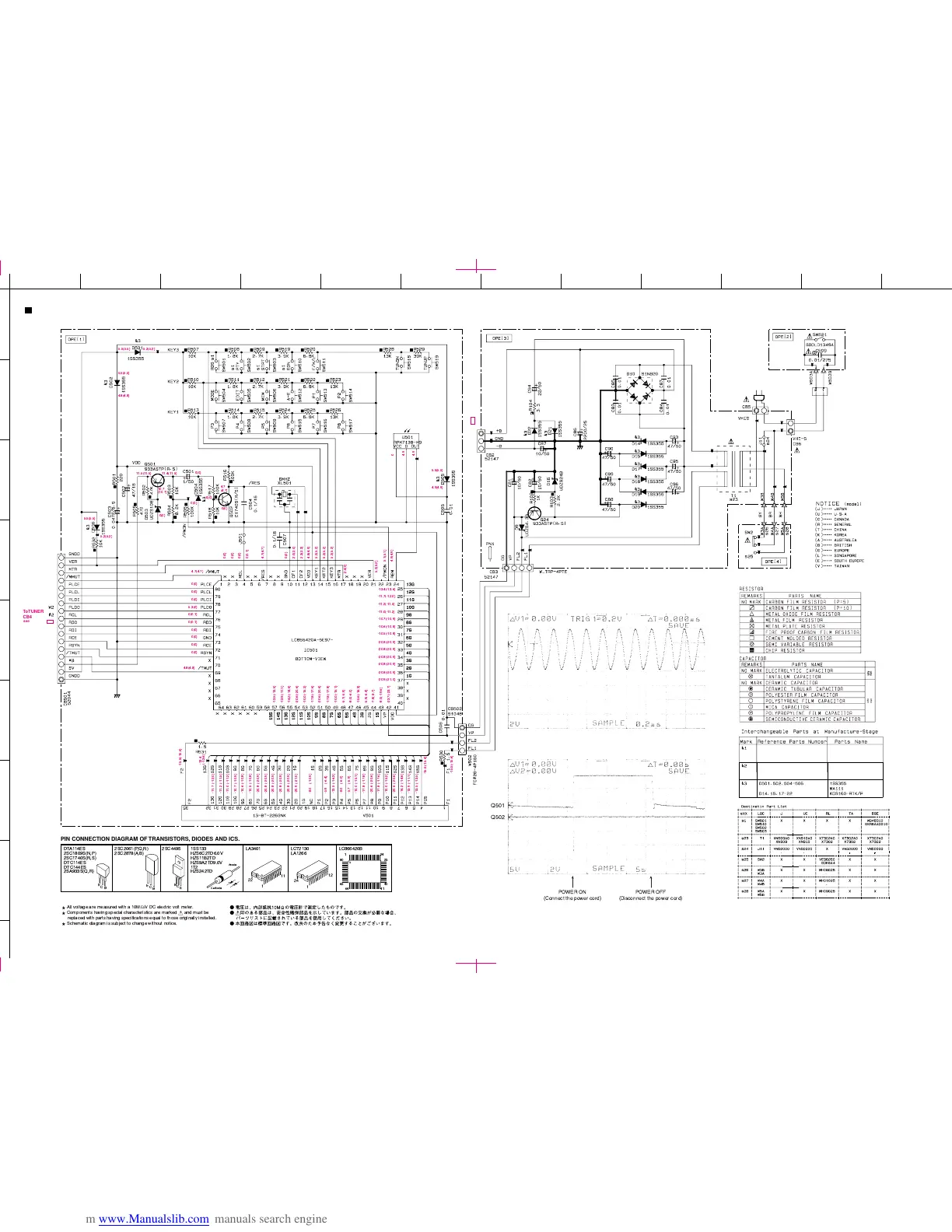
SCHEMATIC DIAGRAM (OPERATION)
pin 12 of IC501
emitter of Q501 and collector of Q502
Q501
Q502
POWER ON
(Connect the power cord)
POWER OFF
(Disconnect the power cord)
PIN CONNECTION DIAGRAM OF TRANSISTORS, DIODES AND ICS.
E
C
B
DTA114ES
2SC1809S(N,P)
2SC1740S(R,S)
DTC114ES
DTC144ES
2SA933S(Q,R)
2SC2061(P,Q,R)
2SC2878(A,B)
2SC4495
B
C
E
1SS133
HZS6C2TD6.0V
HZS11B2TD
HZS9A2TD9.0V
1T2
HZS242TD
Anode
Cathode
LA3401 LC72130
LA1266
LC866420B
1
12
24
1
11
22
64 41
40
25
241
65
80
E
C
B
All voltage are measured with a 10M
Ω
/V DC electric volt meter.
Components having special characteristics are marked
and must be
replaced with parts having specifications equal to those originally installed.
Schematic diagram is subject to change without notice.
5.5(5.5)
5.5(5.5)
5.2(5.2)
5.2(5.2)
11.5(11.5)
11.4(11.5)
10.7
(10.7)
0(0)
0(0)
0(0)
0(0)
0(0)
0(0)
-13.4(-13.6)
-11.7(-12.0)
-11.2(-11.5)
-11.0(-11.2)
-10.7(-10.9)
-10.6(-10.8)
-10.5(-10.8)
-20.8(-20.9)
-20.8(-20.9)
-20.8(-20.9)
-20.8(-20.9)
-20.8(-20.9)
-20.9(-21.0)
)0(0
)0(0
)0(0
)1.0(0
)7.4(7.4
)0(0
)0.2(0.2
)3.2(3.2
)9.4(8.4
)2.5(2.5
)2.5(2.5
)2.5(2.5
)1.5(1.5
)9.
4
(9
.4
9.4
9.4
0
)0(6.2
)2.5(2.5
)7.32-(7.32-
)6.91-(0.8-
)7.3-(8.7-
)4.
6
-(9.5-
)3.61-(6.51-
)0.6-(0.8-
)9.5-(7.5-
)1.51-(0.01-
)8.71-(8.71-
)6.02-(6.02-
)6.71-(8.71-
)2.51-(0.01-
)6.02-(6.02-
-14.2(-14.6)
-13.9(-11.1)
-13.5(-13.5)
)6.51-(5.51-
)6.51-(5.51-
)6.51-(5.51-
)5.11-(2.11-
)2.11-(0.11-
)9.01-(7.01-
)8.01-(6.01-
)8.01-(5.01-
)3.61-(5.31-
)1.51-(0.01-
)2.51-(0.01-
)6.41-(2.41-
)1.11-(9.31-
)5.31-(5.31-
)8.71-(8.71-
)6.71-(8.71-
)6.02-(6.02-
)6.02-(6.02-
)9.02-(8.02-
)9.02-(8.02-
)9.02-(8.02-
)9.02-(8.02-
)9.02-(8.02-
)0.12-(9.02-
)9.01-(0.8-
)0.6-(0.8-
)9.5-(7.
5
-
)4.6-(9.5-
)0.21-(7.11-
4.31-
)6.31-(
0(0)
0(0)
5.3(0)
0(0.1)
0(0.1)
0(0)
0(0)
0(0)
0(0)
4.8(4.8)
4.7
(4.7)
4.7(4.7)
5.5(5.5)
5.5(5.5)
4.9(4.9)
4.8(4.8)
ToTUNER
CB4
see page 21 H7
ToTUNER CB1
see page 21 H3
 Loading...