19
IM 04L55B01-02EN
Terminal Arrangement
M3 screw terminal
CH
No.
Term.
No.
Symbol
Term.
No.
Symbol
Term.
No.
Symbol
CH1
301 B 201 A 101 I
302 C 202 Not not
use
102 C
CH2 303 B 203 A 103 I
CH3
304 B 204 A 104 I
305 C 205 Not not
use
105 C
CH4 306 B 206 A 106 I
CH5
307 B 207 A 107 I
308 C 208 Not not
use
108 C
CH6 309 B 209 A 109 I
310 Not not
use
210 Not not
use
110 Not not
use
Clamp terminal
CH
No.
Term.
No.
Symbol
CH
No.
Term.
No.
Symbol
CH2
201 I
CH1
101 I
202 A 102 A
203 B 103 B
204 C 104 C
205 Not not
use
105 Not not
use
CH4
206 I
CH3
106 I
207 A 107 A
208 B 108 B
209 C 109 C
210 Not not
use
110 Not not
use
CH6
211 I
CH5
111 I
212 A 112 A
213 B 113 B
214 C 114 C
Emptyterminalsmaynotbeused.
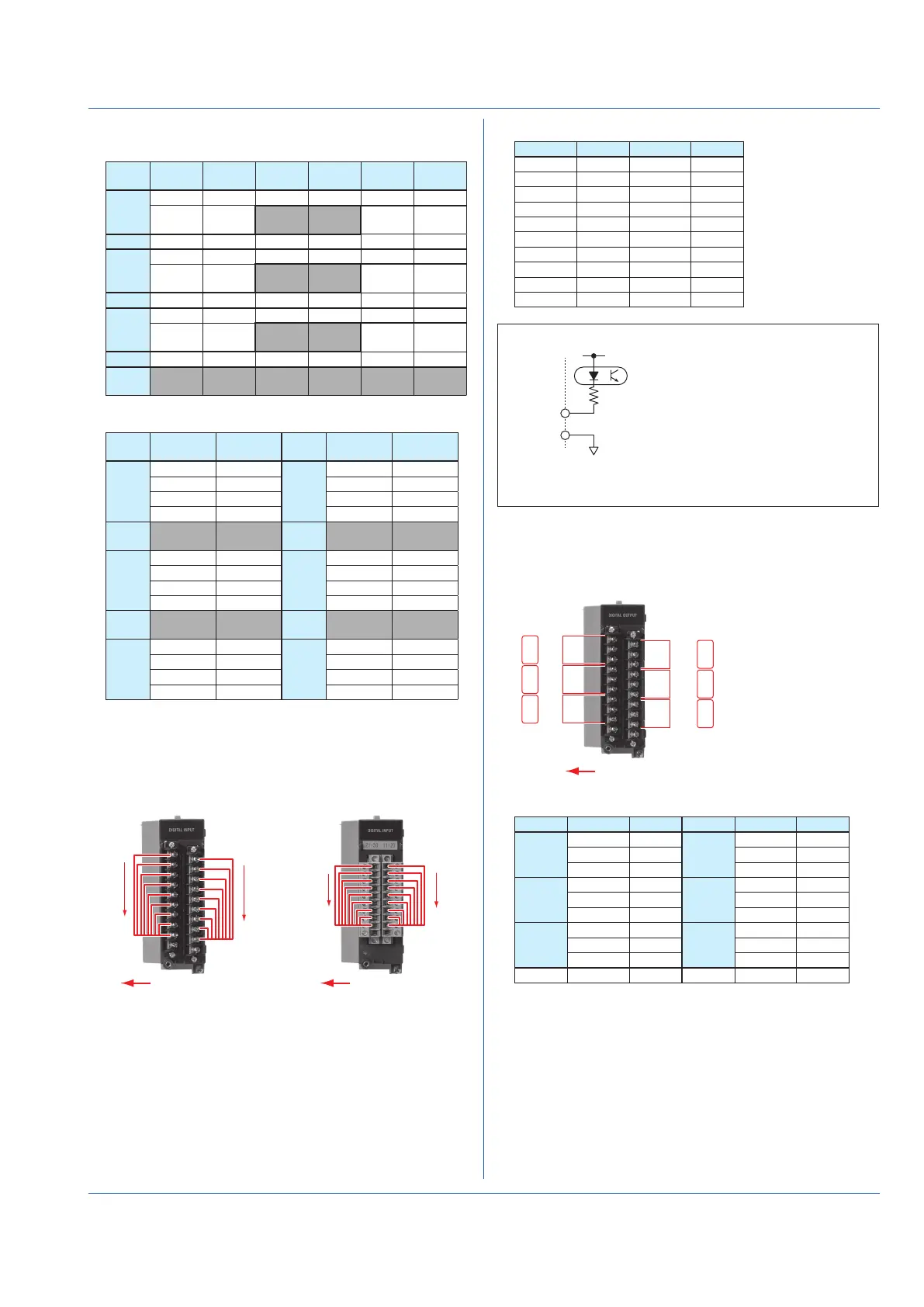
Wiring to a GX90XD Digital Input Module
Terminal Diagram
DI1
M3 screw terminal Clamp terminal
DI8
COM
COM
DI9
DI16
COM
DI9
DI16
DI1
DI8
COM
Wiring direction Wiring direction
(11)
(19)
(11)
(19)
(21)
(29)
(21)
(29)
Terminal Arrangement
Term. No. Symbol Term. No. Symbol
21 DI9 11 DI1
22 DI10 12 DI2
23 DI11 13 DI3
24 DI12 14 DI4
25 DI13 15 DI5
26 DI14 16 DI6
27 DI15 17 DI7
28 DI16 18 DI8
29 COM 19 COM
30 - 20 -
DI1 to
DI16
COM
Input type: Photocoupler isolation
Shared common (COM)
Allowable input voltage range:
0 to 10 V
Note: Do not apply voltage outside
the allowable input voltage
range across input terminals.
Doing so may damage the
GM.
Wiring to a GX90YD Digital Output Module
Terminal Diagram
DO1
N.C.
COM
N.O.
N.C.
COM
N.O.
N.C.
COM
N.O.
N.C.
COM
N.O.
N.C.
COM
N.O.
N.C.
COM
N.O.
M3 screw terminal
DO2
DO3
DO4
DO5
DO6
Wiring direction
11
12
13
14
15
16
17
18
19
21
22
23
24
25
26
27
28
29
Terminal Arrangement
DO No. Term. No. Symbol DO No. Term. No. Symbol
21 NC 11 NC
DO4 22 COM DO1 12 COM
23 NO 13 NO
24 NC 14 NC
DO5 25 COM DO2 15 COM
26 NO 16 NO
27 NC 17 NC
DO6 28 COM DO3 18 COM
29 NO 19 NO
30 - 20 -
 Loading...