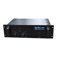
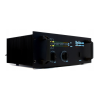
Do you have a question about the Zeck Audio A902 and is the answer not in the manual?
Covers safe service procedures, potential hazards, and component handling guidelines.
Highlights critical components marked for safe operation and replacement instructions.
Displays pin configurations for various transistors used in the amplifier.
Step-by-step guide for adjusting the idle current of the amplifier.
Illustrates the main functional blocks and signal flow of the A902 amplifier.
Provides the detailed schematic diagram of the amplifier's power supply unit.
Shows the detailed schematic of the BIMOS power amplifier output stage.
Details the specific circuitry for the output power block of the amplifier.
Explains the circuit responsible for limiting functions and VU metering.
Illustrates the schematic diagram for the stereo balanced amplifier stage.
| Brand | Zeck Audio |
|---|---|
| Model | A902 |
| Category | Amplifier |
| Language | English |