ZLAC8015 Serco Driver Manual (Special for Hub Servo Motor) V1.0 ZLAC8015 Serco Driver Manual (Special for Hub Servo Motor) V1.0
11 Shenzhen ZhongLing Technology Co.,Ltd. TEL: +86-0755-29799302 FAX:+86-0755-2912 4283 WEB: www.zlingkj.com Shenzhen ZhongLing Technology Co.,Ltd. TEL: +86-0755-29799302 FAX:+86-0755-2912 4283 WEB: www.zlingkj.com 12
3.1.4 DIP switch
Port Pin Mark Name Function
1 SW1
DIP switch
CANOPEN termination
resistance selection
2 SW2 RS485
selection
3 SW3 CANOPEN address selection is
1-3. When it is 0, it can be
set to 4-127 by software.
4 SW4
5 SW5 RS485 address selection is 1-
When it is 0, it can be set to
4-127 by software.
6 SW6
3.1.5 Communication port
Port Pin Mark Name Function
1 CANH CANOPEN
3 CANL
2 A RS485
4 B
5 CANH CANOPEN
7 CANL
6 A RS485
8 B
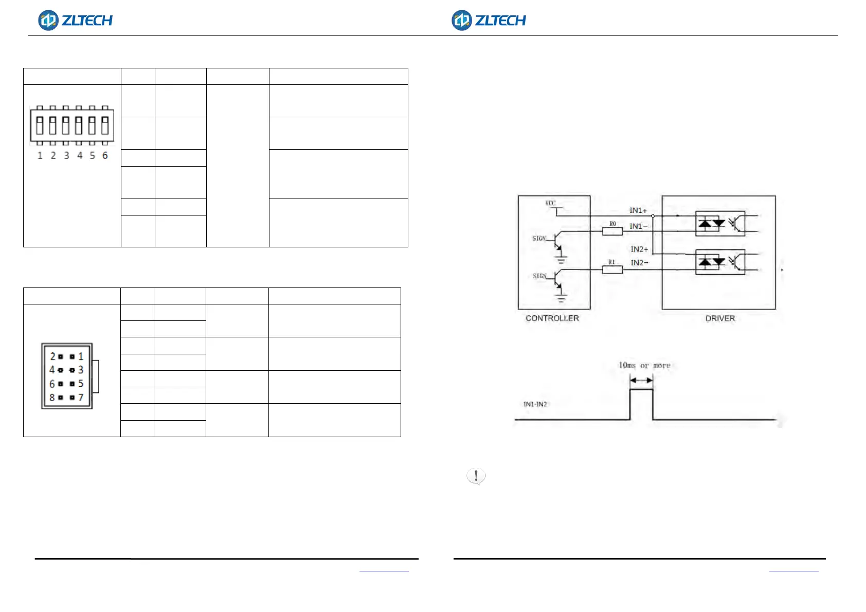
3.2 CONTROL SIGNAL WIRING
ZLAC8015 series driver provides 2 photoelectric isolation programmable input
interfaces, compatible with NPN wiring and PNP wiring.
2-channel (IN1-IN2) programmable input signal is isolated from the external control
interface by an optocoupler. The driver is compatible with common cathode and
common anode connections, as shown in the following Figure 2. In order to ensure the
reliable conduction of the optocoupler inside the driver, the drive current provided by
the controller must be at least 10mA.
The level pulse width of IN1-IN2 input needs to be bigger than 10ms, otherwise the
driver may not respond normally. The IN1-IN2 timing diagram is shown in Figure 3.
Fig.2 Input interface circuit
Fig.3 Control signal interface wiring diagram
Note: The default input voltage of the control signal is 5V. For other voltages,
current limiting resistors must be added, for example: 12V, external 1K 1 / 2W resistor;
24V, external 2K 1 / 2W resistor.
After the driver is powered on, IN1-IN2 defaults to the unspecified state. At this time,
the input signal is invalid. User could configure IN1-IN2 input functions through bus