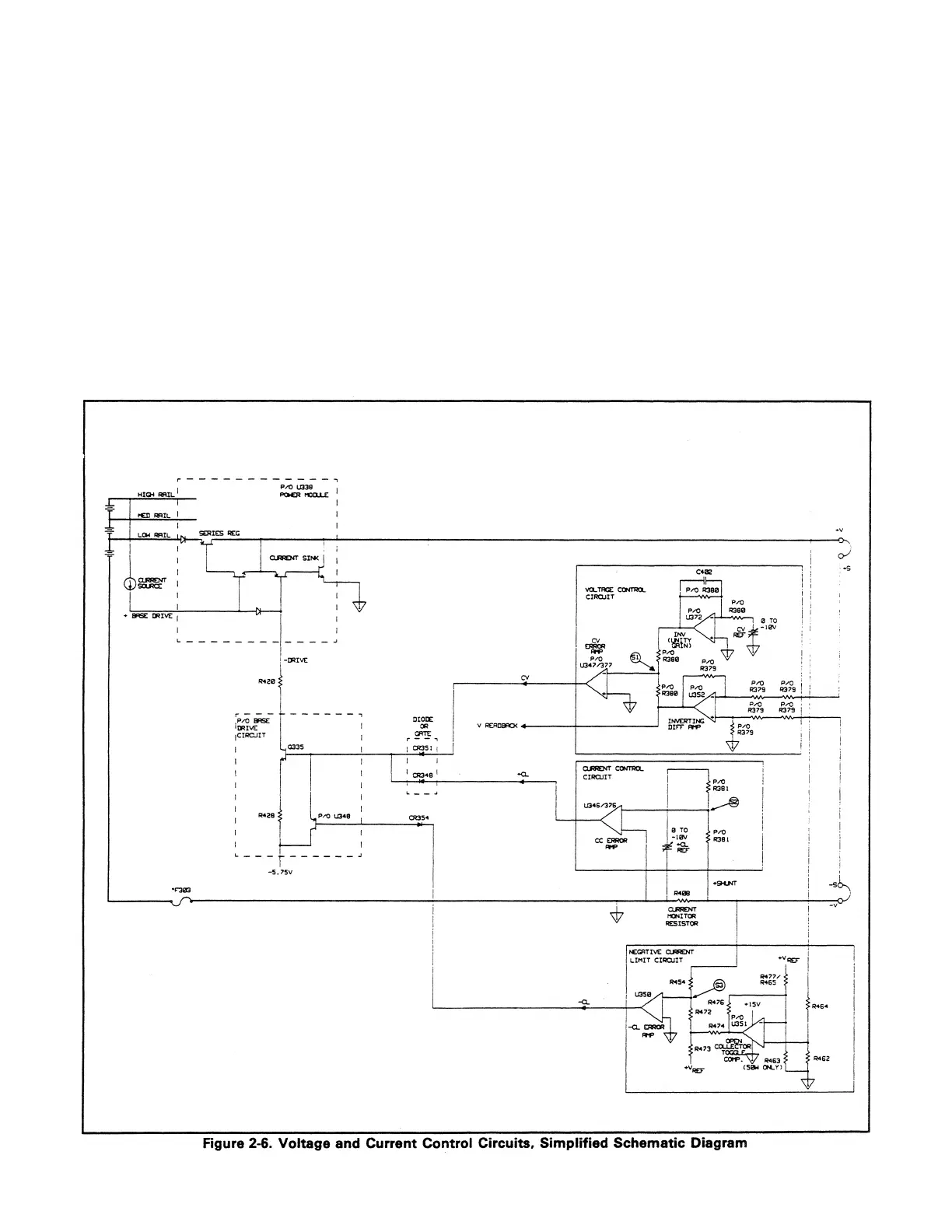
The CV or + CL signal controls the base drive circuit via OR
gate diodes CR351 or CR348 to generate the – DRIVE signal
in order to control the conduction of the series regulators in
the power module and provide a regulated output. If the
output is less than the programmed value, the – DRIVE
signal will allow more + BASE DRIVE current causing the
series regulators to conduct more and raise the output. If the
output exceeds the programmed value, the – DRIVE signal
will divert current through Q335 and U348 of the base drive
circuit and away from the + BASE DRIVE power module
input causing the series regulators to conduct less thereby
reducing the output The voltage control (VV) circuit and the
current control (+CL) circuit is described in paragraphs 2-46
and 2-47, respectively.
When the output is operating in negative current limit, the –
CL signal controls the base drive circuit via diode CR354 so
that the – DRIVE signal controls the conduction of the
current sink transistors in the power module. The negative
current limit circuit which generates the – CL signal is
described in paragraph 2-48. The maximum – Base Drive is
reached when the drop across R428 reaches. 6 volts, turning
on part of U348 which limits the base drive to Q335.
2-46 Voltage Control Circuit. When the output is operating
in the constant voltage mode, this circuit generates the CV
control and CV LOOP signals. The CV control signal is
applied through OR gate diode CR351 to control the base
drive circuit in order to regulate the output voltage. The CV
2-13
Artisan Scientific - Quality Instrumentation ... Guaranteed | (888) 88-SOURCE | www.artisan-scientific.com
 Loading...