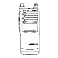
Do you have a question about the Alinco DJ-180 and is the answer not in the manual?
Covers frequency coverage, resolution, memory channels, impedance, signal type, power requirements, dimensions, and weight.
Details output power, modulation system, frequency deviation, tone frequency, DTMF encoder, and tone burst.
Explains receiver system, intermediate frequency, and sensitivity specifications.
Outlines frequency coverage, resolution, memory channels, impedance, signal type, power, dimensions, and weight.
Details output power, modulation system, frequency deviation, tone frequency, timeout timer, and penalty.
Covers receiver system, intermediate frequency, sensitivity, and AF output.
Explains how to activate specific operating modes using key combinations.
Details the double superheterodyne receiver system, including IF frequencies.
Describes the PLL circuit's frequency setting via serial data and VCO tuning.
Details the transmitter's signal path from microphone to antenna.
Explains DTMF signal generation and switching during transmission.
Details the tone squelch decoder and encoder functions.
Refers to terminal functions and covers BS Mode, Backup Reset, and Reset.
Provides test circuit and pinout for the LR408721 tone dialer IC.
Shows the pinout and function for the M5218FP dual op-amp.
Presents the test circuit and pinout for the M5236ML voltage regulator.
Details the function table and pinout of the MB1504LPF frequency synthesizer.
Shows the circuit diagram and pinout for the MC3357 FM IF IC.
Explains the pin functions and operation of the MX365 CTCSS IC.
Shows the circuit and pinout for the NJM386 dual power amplifier.
Details the equivalent circuit and pinout for the RH5VA32AA voltage detector.
Presents the equivalent circuit and pinout for the RH5VA45AA voltage detector.
Shows the pin names and configuration for the X24C01A EEPROM.
Details the pin names and configuration for the X24C04S14 EEPROM.
Presents the pin names and configuration for the X24C16S14 EEPROM.
Shows the COMMON pin connections for the LCD segment display.
Illustrates the SEGMENT pin connections for the LCD display.
Exploded view showing components of the rear case assembly.
Exploded view detailing the components of the LCD assembly.
Exploded view illustrating the components of the second rear case.
Exploded view showing the assembly of the first front case.
Exploded view illustrating the components of the second front case.
Exploded view of the third rear case and battery terminal assembly.
Shows the component layout for the VCO Unit (Side A and Side B).
Details the component layout for the Jack Unit (Side A and Side B).
Displays the component layout for the PTT Unit Side B.
Shows component layouts for the PS Unit (Side A and Side B).
Displays component layout for the ROM1 Unit Side B.
Shows component layout for the ROM2 Unit Side B.
Lists essential test equipment for adjustments, including specs.
Provides instructions on removing screws before performing adjustments.
Details the procedure for PLL adjustment, including test equipment and settings.
Covers TX adjustments for power, deviation, DTMF, and tone burst.
Outlines RX adjustment steps for sensitivity and frequency.
Details the procedure for PLL adjustment for the narrow version.
Covers TX adjustments for power, deviation, DTMF, and tone burst for the narrow version.
Outlines RX adjustment steps for sensitivity and frequency for the narrow version.
Illustrates adjustment points on the RF unit, referring to specific components.
| Type | Handheld Transceiver |
|---|---|
| Modulation | FM |
| Battery | Li-ion 7.4V 1500mAh |
| Voltage | 7.4 V |
| Current drain TX | 1.5 A |
| Antenna Connector | BNC |