EasyManua.ls Logo

Alinco DJ-G5 User Manual

Alinco DJ-G5
73 pages
To Next Page IconTo Next Page
Page #1 background imageLoading...
Page #1 background image
DJ-G5
Service Manual
CONTENTS
+ SPECIFICATIONS
2
+ PARTS LIST
RF Unit 37~40
IF Unit
41
+ CIRCUIT DESCRIPTION CPU Unit 44~46
1) Receiver System 3~5 SVV UniL 46
2) Transmitter System 5 UVCO Unit 46
3) PLL Synthesizer Circuit 6 VVCO Unit 47
4) CPU and Peripheral Circuit 6~7 CHARGE Unit 47
5) Terminal function of CPU 10~12 PTT Unit 47
6) Terminal function of 4094 13 Mechanical Parts 48
7) Frequency Table 13
+ SEMICONDUCTOR DATA
+ ADJUSTMENT
l) AK2341 14 1) Required Test Equipment 49
2) BU4094BF 15 2) Adjustment for DJ-G5T/E 50
3) HD6433877 16 3) Adjustment Points 51
4) LC75366M 17
5) LC73881 M 18
6) M64076GP 19 + PC BOARD VIEW
7) MC3372VM 20 1) RF Unit Side A 52
8) NJM21 00V 20 2) RF Unit Side B 53
9) NJM2070M 21 3) IF Unit Side A 54
10) RH5RH501A 22 4) 1F Unit Side B 55
11) RH5RH651A 22 5) CPU Unit Side A 56
12) S-80730SL-AT 23 6) CPU Unit Side B 57
1 3 )S-AV28 24 7) UVCO Unit 58
14) S-AU57 24 8) VVCO Unit 58
15) S-81237SG-QE 25 9) PTT Unit Side A 58
16) TA75S01F 25 10) PTT Unit Side B 58
17) TA75W01FU 26 11) CHARGE Unit 58
18) TC4W53F 26 12) SW Unit Side A 58
19) TK10930VTL 27
20) uPD1 6430AGF-3B9 28
2 1 )24LC16B 29 + VOLTAGE TABLE
22) Transistor, Diode and LED Outline Dre30 1) Diode 59~60
23) LCD Unit 31~32 2) IC 60~63
3) Transistor 63~64
+ EXPLODED VIEW
1) Charge Unit 33 + BLOCK DIAGRAM 66~67
2) RF Unit 34
3) IF Unit/CPU Unit 35
4) Front/Rear View 36
+ SCHEMATIC DIAGRAM
1) RF Unit 68~69
2) IF Unit 70~71
3) CPU Unit 72~73
4) UVCO Unit 74
5) VVCO Unit 75
6) CHARGE Unit 76
7) PTT Unit 76
ALINCO INCORPORATED
TWIN 21 M.I.D. TOWER BUILDING 23F, 1-61, 2-CHOME,
SHIROMI CHUO-KU , OSAKA, 540-8580 JAPAN
Tel (81)6-6946-8150 fax (81)6-6946-8175
e-mail: export@alinco.co.jp
Question and Answer IconNeed help?

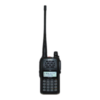
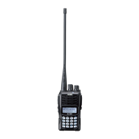
Do you have a question about the Alinco DJ-G5 and is the answer not in the manual?

Alinco DJ-G5 Specifications

General IconGeneral
Channel Capacity200
Battery LifeApprox. 10 hours
Receiver SystemDouble conversion superheterodyne
Current Drain TX1.5 A
Impedance50 ohms
ManufacturedJapan
ModulationFM, AM
Voltage7.2 VDC
Frequency Range TX144-146 MHz, 430-440 MHz

Summary

CIRCUIT DESCRIPTION

1) Receiver System

Details the double-conversion superheterodyne receiver system.

3 Demodulation

Explains signal demodulation for L and R bands, FM and AM.

4 Audio Circuit

Describes audio signal processing, pre-emphasis, volume control, and amplification.

2) Transmitter System

Explains voice conversion, pre-emphasis, power amplification, and APC circuit.

2 Power Amplifier

Details pre-drive, drive, and power modules for transmitting signal amplification.

3 APC Circuit

Explains voltage detection and control for fixing transmitting power.

3) PLL Synthesizer Circuit

Describes PLL IC, reference frequency division, phase comparison, and VCO circuits.

4) CPU and Peripheral Circuit

Covers CPU functions, LCD display, and related peripheral circuits.

5) Terminal function of CPU

Continues detailed pin functions for CPU, covering various inputs and outputs.

SEMICONDUCTOR DATA

1) AK2341 (XA0239)

CTCSS Encoder/Decoder pinout, function, and block diagram.

3) HD6433877 (XA0505)

CPU pinout and description.

EXPLODED VIEW

1) Charge Unit

Lists parts and assembly for the charge unit.

2) RF Unit

Lists parts and assembly for the RF unit.

3) IF Unit/CPU Unit

Lists parts and assembly for IF and CPU units.

PARTS LIST

ADJUSTMENT

1) Required Test Equipment

Lists necessary test equipment for adjustments.

2) Adjustment for DJ-G5T/E

Provides detailed adjustment procedures and parameters for specific models.

3) Adjustment Points

Illustrates the locations of adjustment potentiometers on the IF and RF units.

PC BOARD VIEW

VOLTAGE TABLE

Transistor

3) Transistor

Continues transistor data, including specific models and operating conditions.

BLOCK DIAGRAM

System Block Diagram Overview

Illustrates the overall functional blocks and their interconnections.

SCHEMATIC DIAGRAM

1) RF UNIT

Shows detailed circuit schematics for the RF unit.

2) IF UNIT

Shows detailed circuit schematics for the IF unit.

3) CPU UNIT

Continues detailed circuit schematics for the CPU unit.

4) UVCO UNIT

Shows detailed circuit schematics for the UVCO unit.

5) VVCO UNIT

Shows detailed circuit schematics for the VVCO unit.

6) CHARGE UNIT

Shows detailed circuit schematics for the CHARGE unit.

7) PTT UNIT

Shows detailed circuit schematics for the PTT unit.

Related product manuals