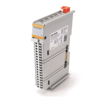
4 FLEX™ I/O Isolated Input/Output Analog Module
Publication 1794-IN039F-EN-P - November 2011
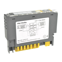
Status Indicator
The OK status indicator is two-colored: red and green. The indicator flashes green
for one of three reasons:
1. The module configuration word is zero (for example, power up reset
condition).
2. The 24V DC user power is off.
3. The module is in configuration mode.
The indicator displays red to indicate that the module did not pass the initial
hardware test. Cycle power again.
After power up, if the status indicator is not flashing green or solid green, cycle
module power once more to verify a proper reset of the bus interface.
Specifications
Word 4 Output channel 1
configuration
Output channel 0
configuration
Input channel 1
configuration
Input channel 0
configuration
Word 5 0 Real time sample programmed interval
Word 6 IC 1 TR IT Q1 Q0 0 0 RV QK CK GO Channel number
Where: EN = Output enable bit
S0 and S1 = Safe state source bits
TR = Transparent bit
IT = Interrupt toggle bit
IC = Initiate configuration bit
Q0 and Q1 = Requests for outputs to hold
RV = Revert to defaults bits
QK = Quick calibration
CK = Calibration clock
oGO = Gain offset select
Configure the Input Channels
Input Channel Configuration
03 02 01 00 Set these bits for channel 0
07 06 05 04 Set these bits for channel 1
Configuration Bits Nominal Range Data Type % Underrange
% Overrange
Output Values
MSD LSD
0 0 0 1 4...20 mA Signed 2’s
complement
4% under; 4% over <0000…7878>
0 0 1 0 ±10V 2% under; 2% over <831F…7CE1>
0 0 1 1 ±5V 4% under; 4% over <8618…79E8>
0 1 0 0 0...20 mA Signed 2’s
complement %
0% under; 4% over <0…10000>
0 1 0 1 4…20 mA 4% under; 4% over <0…10000>
0 1 1 0 0…10V 0% under; 2% over 0…10000
0 1 1 1 ±10V 2% under; 2% over <-10000…10000>
1 0 0 0 0…20 mA Binary 0% under; 4% over 0000…F3CF
1 0 0 1 4…20 mA 4% under; 4% over 0000…F0F1
1 0 1 0 0…10V 0% under; 2% over 0000…F9C2
1 0 1 1 0…5V 0% under; 4% over 0000…F3CF
1 1 0 0 ±20 mA Offset binary,
8000H = 0 mA
4% under; 4% over <8000…F9E8>
1 1 0 1 4…20 mA Offset binary,
8000H = 4 mA
4% under; 4% over <8000…F878>
1 1 1 0 ±10V Offset binary,
8000H = 0 V
2% under; 2% over <031F…FCE1>
1 1 1 1 ±5V 4% under; 4% over <0618…F9E8>
Update Rate for Real Time Sample Interval = 0
Configuration Bits Nominal Ranges
Channel Update Rate
(1)
MSD LSD
RTSI = 0 and No Low
Pass Filter
RTSI and Filter = 0
IT Bit = 1
0 0 0 1 4...20 mA 7.5 ms 5.0 ms
0 0 1 0 ±10V 2.5 ms 2.5 ms
0 0 1 1 ±5V 2.5 ms 2.5 ms
0 1 0 0 0...20 mA 7.5 ms 5.0 ms
0 1 0 1 4…20 mA 7.5 ms 5.0 ms
0 1 1 0 0…10V 5.0 ms 5.0 ms
0 1 1 1 ±10V 5.0 ms 5.0 ms
1 0 0 0 0…20 mA 2.5 ms 2.5 ms
1 0 0 1 4…20 mA 7.5 ms 5.0 ms
1 0 1 0 0…10V 2.5 ms 2.5 ms
1 0 1 1 0…5V 2.5 ms 2.5 ms
1 1 0 0 +20 mA 2.5 ms 2.5 ms
1 1 0 1 4…20 mA 7.5 ms 5.0 ms
1 1 1 0 ±10V 2.5 ms 2.5 ms
1 1 1 1 ±5V 2.5 ms 2.5 ms
(1)
When IT = 1, the channel update rate for all channels is determined by the slowest channel.
Output Map
Dec 1514131211109876543210
Oct 17161514131211107 6 5 4 3 2 1 0
Set the Input Filters
Input Channel Filter
03 02 01 00 Set these bits for channel 0
07 06 05 04 Set these bits for channel 1
Bit Settings A/D Conversion Rate Low Pass Filter
0 0 0 0 1200 Hz No low pass
0 0 0 1 1200 Hz 100 ms low pass
0 0 1 0 1200 Hz 500 ms low pass
0 0 1 1 1200 Hz 1000 ms low pass
0 1 0 0 600 Hz No low pass
0 1 0 1 600 Hz 100 ms low pass
0 1 1 0 600 Hz 500 ms low pass
0 1 1 1 600 Hz 1000 ms low pass
1 0 0 0 300 Hz No low pass
1 0 0 1 300 Hz 100 ms low pass
1 0 1 0 300 Hz 500 ms low pass
1 0 1 1 300 Hz 1000 ms low pass
1 1 0 0 150 Hz No low pass
1 1 0 1 150 Hz 100 ms low pass
1 1 1 0 150 Hz 500 ms low pass
1 1 1 1 150 Hz 1000 ms low pass
Configure the Output Channels
Output Range Selection and Update Rate
11 10 09 08 Set these bits for channel 0
15 14 13 12 Set these bits for channel 1
Configuration Bits Nominal Range Data Type Output Values Module Update
Rate
MSD LSD
0 0 0 1 4...20 mA Signed 2’s
complement
<0000…7878> 5.0 ms
0 0 1 0 ±10V <8618…79E8 2.5 ms
0 0 1 1 ±5V <8618…79E8> 2.5 ms
0 1 0 0 0...20 mA Signed 2’s
complement %
0…10000> 5.0 ms
0 1 0 1 4…20 mA <0…10000> 5.0 ms
0 1 1 0 0…10V 0…10000 5.0 ms
0 1 1 1 ±10V <-10000…10000> 5.0 ms
1 0 0 0 0…20 mA Binary 0000…F3CF 2.5 ms
1 0 0 1 4…20 mA 0000…F0F1 5.0 ms
1 0 1 0 0…10V 0000…F3CF 2.5 ms
1 0 1 1 0…5V 0000…F3CF 2.5 ms
1 1 0 0 0…20 mA Offset binary <8000…F9E8> 2.5 ms
1 1 0 1 4…20 mA <8000…F878> 5.0 ms
1 1 1 0 ±10V <0618…F9E8> 2.5 ms
1 1 1 1 ±5V <0618…F9E8> 2.5 ms
General Specifications
Attribute Value
Module location 1794-TB2, 1794-TB3, 1794-TB3S, 1794-TB3T, 1794-TB3TS, or 1794-TBN
terminal base.
FlexBus voltage 5V DC
FlexBus current 50 mA
External DC power supply,
nom voltage range
24V DC
19.2…31.2V DC (includes 5% AC ripple)
External DC power supply
current
150 mA @ 24V DC
Thermal dissipation, max 11.3 BTU/hr @ 31.2V DC
Power dissipation, max 3.3 W @ 31.2V DC
 Loading...