DE1-SOC COMPUTER SYSTEM WITH NIOS II For Quartus II 15.0
3190
. . .
123
. . .
. . .
. . .
. . .
0
1
2
. . .
239
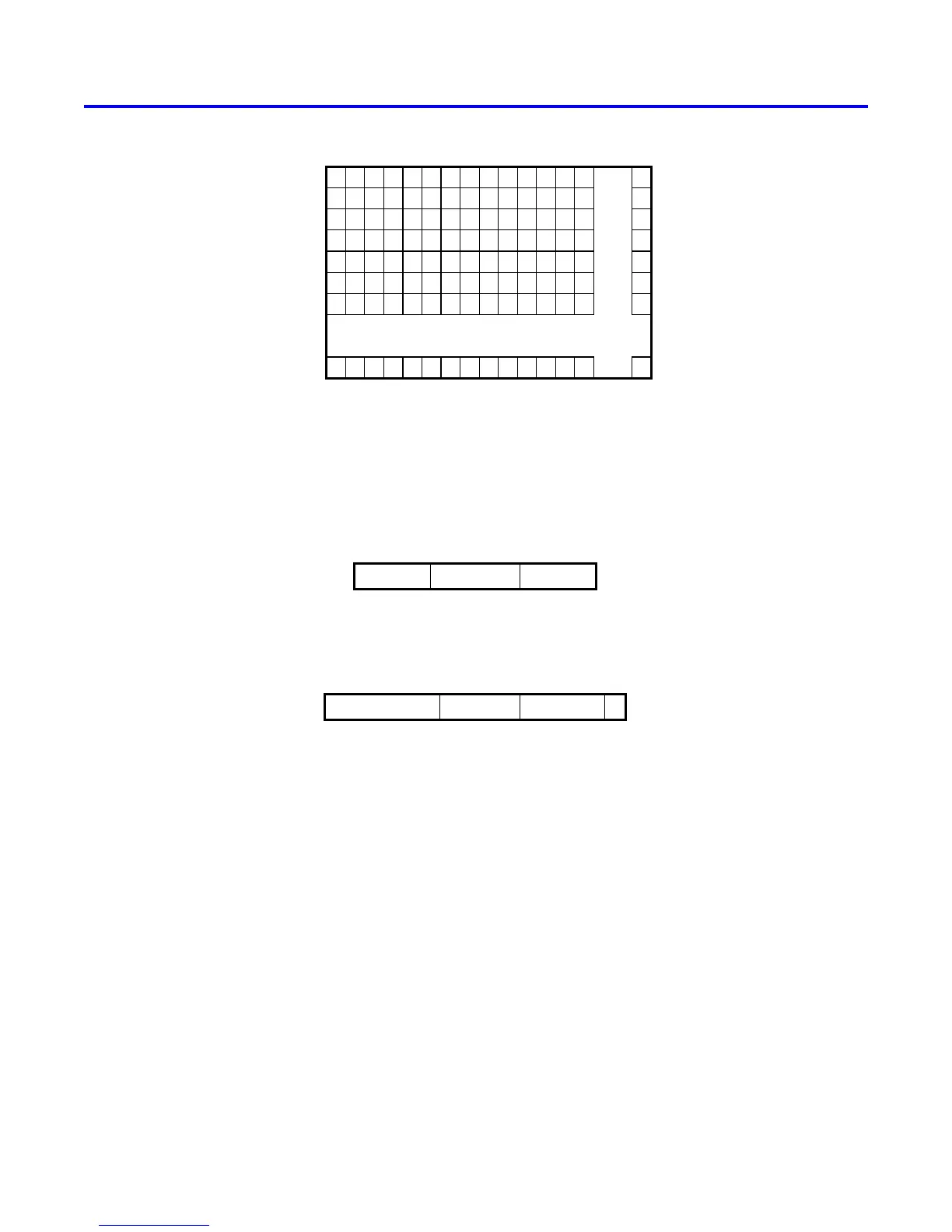
Figure 27. Pixel buffer coordinates.
= (08000002)
16
, the pixel 0,1 has the address base + (00000001 000000000 0)
2
= (08000400)
16
, and the pixel at
location 319,239 has the address base + (11101111 100111111 0)
2
= (0803BE7E)
16
.
31
. . .
1
. . .
1017
00001000000000
918
xy
. . .
(a) Pixel values
(b) Pixel buffer addresses
0
0
15
. . .
0
. . .
510
red
411
bluegreen
. . .
Figure 28. Pixel values and addresses.
You can create an image by writing color values into the pixel addresses as described above. A dedicated pixel buffer
controller continuously reads this pixel data from sequential addresses in the corresponding memory for display on
the VGA screen. You can modify the pixel data at any time, simply by writing to the pixel addresses. Thus, an
image can be changed even when it is in the process of being displayed. However, it is also possible to avoid making
changes to the pixel buffer while it is being displayed, by using the concept of double-buffering. In this scheme, two
pixel buffers are involved, called the front and back buffers, described below.
4.2.2 Double Buffering
As mentioned above, a pixel buffer controller reads data out of the pixel buffer so that it can be displayed on the
VGA screen. This pixel buffer controller includes a programming interface in the form of a set of registers, as
illustrated in Figure 29. The register at address 0xFF203020 is called the Buffer register, and the register at address
Altera Corporation - University Program
2015
33