DE1-SOC COMPUTER SYSTEM WITH NIOS II For Quartus II 15.0
0xFF203024 is the Backbuffer register. Each of these registers stores the starting address of a pixel buffer. The
Buffer register holds the address of the pixel buffer that is displayed on the VGA screen. As mentioned above, in
the default configuration of the DE1-SoC Computer this Buffer register is set to the address 0x08000000, which
points to the start of the FPGA on-chip memory. The default value of the Backbuffer register is also 0x08000000,
which means that there is only one pixel buffer. But software can modify the address stored in the Backbuffer
register, thereby creating a second pixel buffer. An image can be drawn into this second buffer by writing to its pixel
addresses. This image is not displayed on the VGA monitor until a pixel buffer swap is performed, as explained
below.
A pixel buffer swap is caused by writing the value 1 to the Buffer register. This write operation does not directly
modify the content of the Buffer register, but instead causes the contents of the Buffer and Backbuffer registers to
be swapped. The swap operation does not happen right away; it occurs at the end of a VGA screen-drawing cycle,
after the last pixel in the bottom-right corner has been displayed. This time instance is referred to as the vertical
synchronization time, and occurs every 1/60 seconds. Software can poll the value of the S bit in the Status register,
at address 0xFF20302C, to see when the vertical synchronization has happened. Writing the value 1 into the Buffer
register causes S to be set to 1. Then, when the swap of the Buffer and Backbuffer registers has been completed S is
reset back to 0.
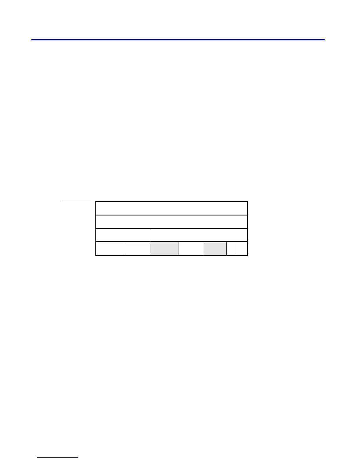
Address
01531 . . .
0xFF203020
0xFF203024
. . .
AS
1
XY
16 223
front buffer address
0xFF203028
back buffer address
0xFF20302C
3
B
. . .7
mn
48. . .24
Backbuffer register
Resolution register
Status register
Buffer register
Unused Unused
Figure 29. Pixel buffer controller registers.
In a typical application the pixel buffer controller is used as follows. While the image contained in the pixel buffer
that is pointed to by the Buffer register is being displayed, a new image is drawn into the pixel buffer pointed to by
the Backbuffer register. When this new image is ready to be displayed, a pixel buffer swap is performed. Then, the
pixel buffer that is now pointed to by the Backbuffer register, which was already displayed, is cleared and the next
new image is drawn. In this way, the next image to be displayed is always drawn in the “back” pixel buffer, and the
two pixel buffer pointers are swapped when the new image is ready to be displayed. Each time a swap is performed
software has to synchronize with the VGA controller by waiting until the S bit in the Status register becomes 0.
As shown in Figure 29 the Status register contains additional information other than the S bit. The fields n and m
give the number of address bits used for the X and Y pixel coordinates, respectively. The B field specifies the number
of bytes used for each pixel, with the minimum being 1 and the maximum 4. The A field allows the selection of
two different ways of forming pixel addresses. If configured with A = 0, then the pixel controller expects addresses
to contain X and Y fields, as we have used in this section. But if A = 1, then the controller expects addresses to be
consecutive values starting from 0 and ending at the total number of pixels−1.
In Figure 28b the default values of the status register fields in the DE1-SoC Computer are used when forming
34 Altera Corporation - University Program
2015
 Loading...


