Bank MIO # Device Signal I/O Notes
GPIO
24 MDIO LPD_MIO24_GEM_MDC O GEM MD clock
25 LPD_MIO25_GEM_MDIO I/O GEM MD I/O
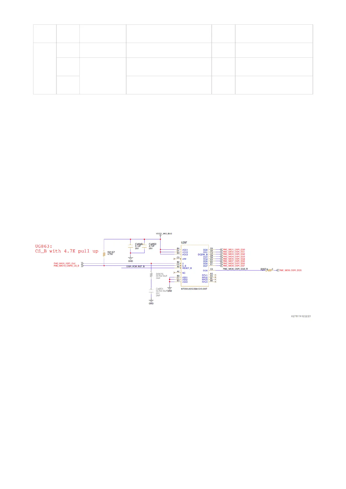
PMC MIO[0–10,12] Bank 500: OSPI U297
[Figure 1, callout 38]
The VEK280 evaluation board uses one Micron MT35XU02GCBA1G12-0SIT 8-bit
serial peripheral interface (octal SPI) flash device. This 2 Gb NOR flash device can
be used as onboard boot, as well as non-volatile storage memory. When used as a
boot source, it is selectable from SW1. See Switches for more information.
See schematic page 28.
Figure: Dual Parallel OSPI Circuit
PMC MIO[13:25] Bank 500: USB 2.0 ULPI PHY
The VEK280 evaluation board uses a Standard Microsystems Corporation USB3320
USB 2.0 ULPI transceiver (U99) to support a USB 2.0 type-A connector (J308). The
USB3320 is a high-speed USB 2.0 PHY supporting the UTMI+ low pin interface
(ULPI) interface standard. The ULPI standard defines the interface between the USB
controller IP and the PHY device, which drives the physical USB signaling. Using the
ULPI standard reduces the interface pin count between the USB controller IP and
the PHY device.
The USB3320 is clocked by a 24 MHz crystal (X8). See the Standard Microsystems
Corporation (SMSC) USB3320 data sheet for clocking mode details. The interface
to the USB3320 PHY is implemented through the IP in the XCVE2802 device PS.