peripherals. This interface is used for the SD boot mode and supports SD2.0 and
SD3.0 access.
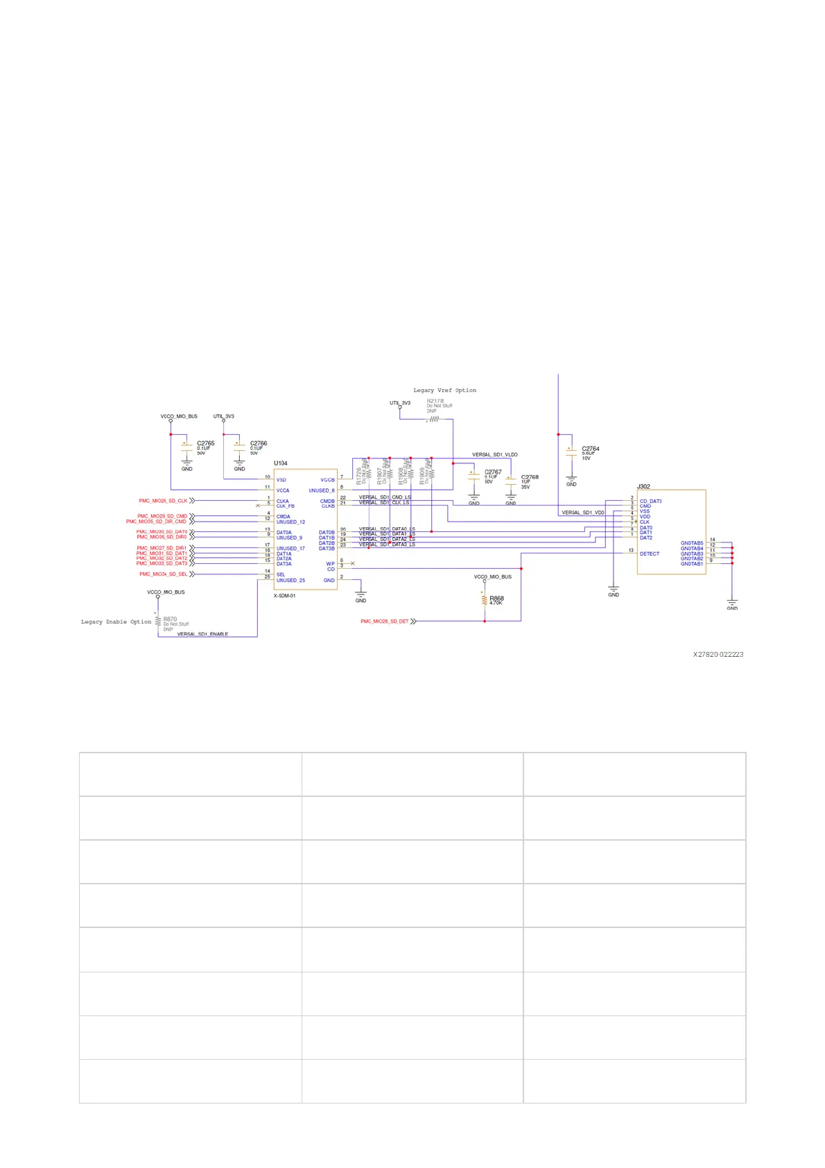
The SDIO interface signals PMC_MIO[26:36, 51] are connected to XCVE2802 device
bank 501, which has its VCCO set to 1.8V. Six SD interface nets PMC_MIO[26, 29,
30:33] are passed through a NXP NVT4857UK SD 3.0-compliant voltage level-
translator U104. This translator is present between the Versal device and the SD
card connector (J302). The NXP NVT4857UK U104 device provides SD3.0 capability
with SDR104 performance. The following figure shows the connections of the SD
card interface on the VEK280 evaluation board.
Figure: SD Card Interface Connections
The following table lists the NVT4857UK U104 adapter pinout.
Table: NVT4857UK U104 Adapter Pinout
Aries Adapter Pin Number NVT4857UKAZ Pin NumberNVT4857UKAZ Pin Name
1 D2 CLKA
2 C3, C2 GND
3 B2 CD
4 C1 CMDA
5 E2 CLK_FB
6 Unused Unused
7 B3 VCCB