1112
Assembly Instructions
PC Board Preparations:
I know that you are more than ready to go, so lets start off by pre p a r i n g
the printed circuit boards, (PCB’s ) .
Locate the “panelized” PCB and break them apart by twisting the board
or cutting at the bridging tabs, producing 5 separate printed circ u i t
b o a rd s .
The 5 boards are as follows;
q Main PCB (the largest one),
q Left CH Filter Bank,
q Main Filter Bank,
q AC SW PCB,
q Right CH Filter Bank.
Using your file - debur the edges of all the boards where the bridging
tabs have left a jagged broken edge.
Then get ready to really start the assembly of your new SET- 3 0 0 B
a m p l i f i e r. This is where you create those plumes of solder resin smoke,
which seems to lull you into your own private world. You know that
entrancing state that your mind invariably takes you to when you dwell so
deeply into the concentration of building something with your own
hands... Let these thoughts flow through your mind now, turn on your
soldering iron, and here we go!
PC Board Stuffing:
Please note that with the exception of the tube sockets and their
s t a n d o ffs, all components mount on the silk-screened side of any of the
PC boards. Outlines for components are silk-screened on the PC board
to aid in the part identification and to facilitate the correct placement of
the components. Remember that the re f e rence designators are also
included in the Parts List on page 4.
Following the stuffing sequence guide below, you simply obtain the bag
containing the appropriate part, carefully bend the leads, place them into
the holes in the PC board, and solder into place. Trim the leads from the
rear side and that is it! Repeat this process several times, and the
b o a rds will be stuffed. Assembly proceeds in this ord e r.
Rectifier Diodes & Bridges:
Ve ry import a n t : the band on the diodes must correspond to the band
on the diode outline on the PC board .
q D1,2 LD1,2 S F 4 0 0 7
Installing these Bridge Rectifiers correctly add an extra challenge, are
you up to it? CUE: Look for the “+” sign on the part to align with the PCB
m a r k i n g s .
q BR100, LBR100 TL400G
(Keep these cut leads they will be used later. )
q BR400 R B 1 5 1
Resistors:
I m p o rtant: Resistors identified with an asterisk “*” should be raised off the
PC board surface by approximately 3/16” (or 4mm), in order to aid heat
dissipation of that part .
Resistors: (Keep some of these small resistor leads for later use.)
q R1, LR1 100K Holco (Black w/white lettering)
q R2, LR2 1K (Sig)
q R3, LR3 475R (Sig)
q R5,8, LR5,8 100R Holco (Black w/white lettering) (Sig)
q R10, LR10 249K (Sig)
q R11,12, LR11,12 100R Metal Film (coloured stripes)
q R301,302, R400,401 100R Metal Film (coloured stripes)
q RF1 1 K 2
q VR1, LVR1 200R Trimpot - (Tu rn the trimmer pots to
their center position if they are not there alre a d y. )
Next these are all - raised above PCB 3/16” (4mm)!
q R4, LR4 33K 2W* (Sig)
q R209A, B, LR209A, B 68K 2W* On Left & Right CH Filter Banks
q R300 100K 2W*
q R210, LR210 150K 2W* On Left & Right CH Filter Banks
q R205A,B, R206A,B 220K 2W* On Main Filter Bank
q R208A,B, LR208A,B 220K 2W* On Left & Right CH Filter Banks
q R6, LR6 10K 3W* (Sig)
q R200, R201, R202, R203 5R6 3W*
q R13, R13A, LR13, LR13A 3K9 5W*
q R13, B, C, LR13,B, C 3K 5W*
q R7, LR7 10K 5W*
q R207, LR207 1K 5W* On Left & Right CH Filter Banks
q R402, 9B, LR9A, B 15K 5W*
q R100,101 LR100,101 .56R 5W*
8-Pin Tube Socket Installation on the Main PCB:
As noted above, all of the tube sockets will be mounted on the rear side
of the Main PCB. (The side with no white silk-screening on it). Notice the
labeling on the PCB -”REAR SIDE SOCKET”.
You will need to gather these part s :
q 8 Pin PCB Mount Octal Sockets x5
q 4-40 x 1/4” Philips scre w, Pan head x 2 0
q #4 Internal tooth lock washer x 1 0
q 4-40 1/2” Hex. Aluminum Stand-off x 1 0
q As a sub-assembly, loosely screw the standoff’s to each of the octal
sockets using the 4-40 screws, (no washers used here). The 2 standoff’s
point in the same direction as the socket pins.
Note that there is only ONE electrically correct orientation for these
8-pin sockets when placed into the PC board. Each socket has a central
hole with a notch groove. This is the indexing keyway, which must line up
with the silk-screen outline on the topside of the PC board .
q Now place the socket assemblies in their appropriate locations - do not
solder yet!
q F rom the component side, secure the socket sub-assembly to the PCB
with the 4-40 screws and #4 lock washers.
q Tighten up the screws to hold the tube sockets securely to the stand-
o ffs. You may need to hold the standoff’s secure as you tighten the
s c re w s .
q Check again that the tube sockets are aligned pro p e r l y. Now is the
time to solder the socket pins to the PCB.
q Once the sockets have been soldered to the PC board, the ends of the
pins can be trimmed.
Capacitors - Electrolytic:
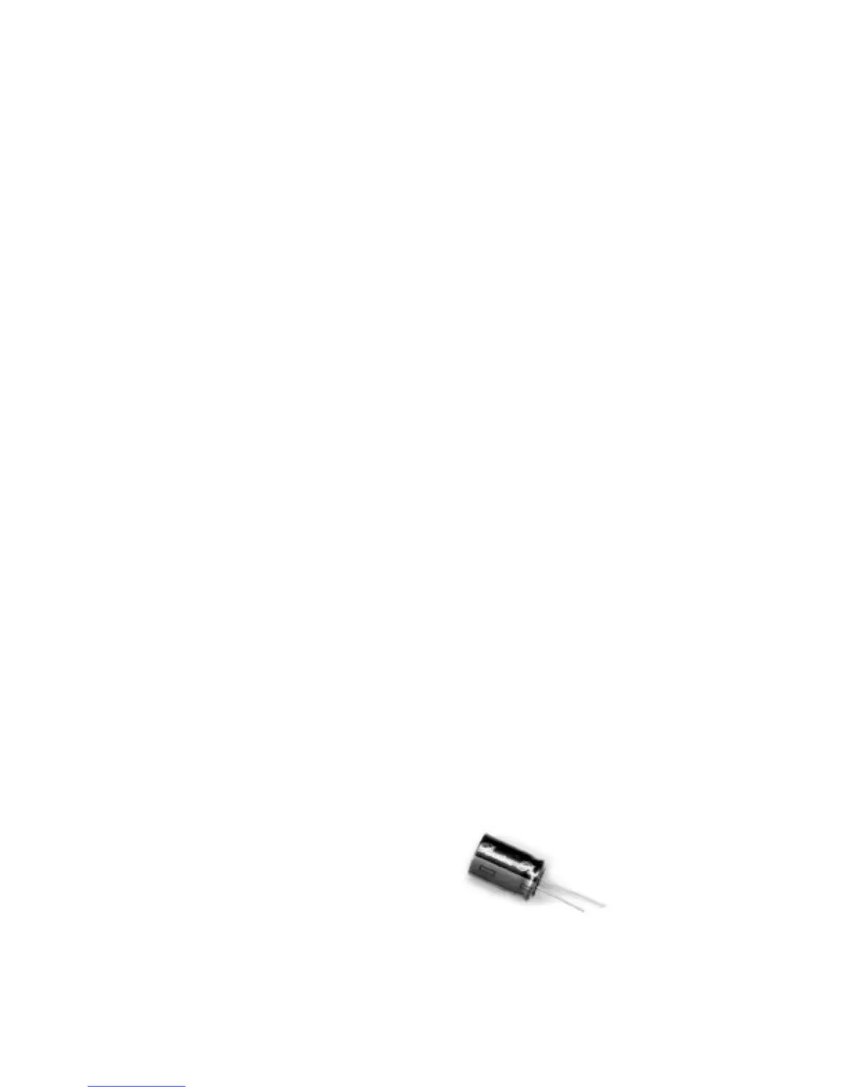
Did you know that electrolytic caps are polarity sensitive? Yes they are ,
and do you know what happens to them if you put them in backward s ?
Nothing, not until you apply power to them that is, then they BLOW UP in
a big puff of smoke!!! No kidding, so please take note of the picture that
shows the cap polarity. Look at the caps, the NEGATIVE leads or
t e rminals are all marked with a large wide band with a negative sign in it.
This then means that the opposite lead or terminal will be the POSITIVE
one. Align the Positive with the “+” sign on the PCB. Get this wrong and
your neighbours may end up knowing about it when they see the smoke
signals emanating from your work shop window.
+
–
 Loading...