EasyManua.ls Logo

Atmel 8051 User Manual

Atmel 8051
113 pages
To Next Page IconTo Next Page
To Previous Page IconTo Previous Page
Page #82 background imageLoading...
Page #82 background image
Common Features Description
2-81 Atmel 8051 Microcontrollers Hardware Manual
4316B–8051–02/04
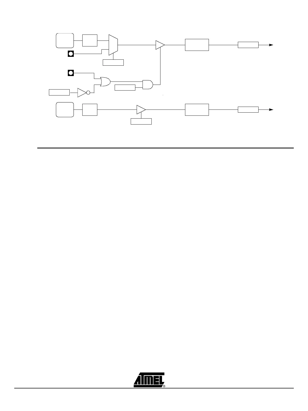
Figure 2-12. Timer/Counter 0 in Mode 3: Two 8-bit Counters
2.11 Timer 1 Timer 1 is identical to timer 0, except for mode 3, which is a hold-count mode. The fol-
lowing comments help to understand the differences:
Timer 1 functions as either a timer or event counter in three modes of operation.
Figure 2-9 to Figure 2-11 show the logical configuration for modes 0, 1, and 2. Timer
1’s mode 3 is a hold-count mode.
Timer 1 is controlled by the four high-order bits of the TMOD register (see Table 2-5
on page 82) and bits 2, 3, 6 and 7 of the TCON register (see Table 2-3 on page 83).
The TMOD register selects the method of timer gating (GATE1), timer or counter
operation (C/T1#) and mode of operation (M11 and M01). The TCON register
provides timer 1 control functions: overflow flag (TF1), run control bit (TR1), interrupt
flag (IE1) and interrupt type control bit (IT1).
Timer 1 can serve as the baud rate generator for the serial port. Mode 2 is best
suited for this purpose.
For normal timer operation (GATE1 = 0), setting TR1 allows TL1 to be incremented
by the selected input. Setting GATE1 and TR1 allows external pin INT1# to control
timer operation.
Timer 1 overflow (count rolls over from all 1s to all 0s) sets the TF1 flag generating
an interrupt request.
When timer 0 is in mode 3, it uses timer 1s overflow flag (TF1) and run control bit
(TR1). For this situation, use timer 1 only for applications that do not require an
interrupt (such as a baud rate generator for the serial port) and switch timer 1 in and
out of mode 3 to turn it off and on.
It is important to stop timer/counter before changing modes.
2.11.1 Mode 0 (13-bit
Timer)
Mode 0 configures Timer 1 as a 13-bit timer, which is set up as an 8-bit timer (TH1 reg-
ister) with a modulo-32 prescaler implemented with the lower 5 bits of the TL1 register
(see Figure 2-9). The upper 3 bits of the TL1 register are ignored. Prescaler overflow
increments the TH1 register.
TR0
TCON.4
TF0
TCON.5
INT0#
0
1
Overflow
Timer 0
Interrupt
Request
C/T0#
TMOD.2
TL0
(8 bits)
TR1
TCON.6
TH0
(8 bits)
TF1
TCON.7
Overflow
Timer 1
Interrupt
Request
T0
PERIPH
CLOCK
÷ 6
PERIPH
CLOCK
÷ 6
GATE
Question and Answer IconNeed help?

Do you have a question about the Atmel 8051 and is the answer not in the manual?

Atmel 8051 Specifications

General IconGeneral
Architecture8-bit
Serial CommunicationUART
CPU8051
Program MemoryUp to 64 KB Flash
Timers/Counters2 or 3 (16-bit)
SPIYes
I2CYes
ADCYes (some variants)
Operating Voltage2.7V to 5.5V
Operating Temperature-40°C to +85°C
PackageDIP, PLCC, TQFP

Summary

Section 1: The 8051 Instruction Set

1.1 Program Status Word

Details the Program Status Word (PSW) register, its bits, and their functions.

1.2 Addressing Modes

Describes the various addressing modes used by the 8051 instruction set.

1.3 Arithmetic Instructions

Lists and explains the arithmetic instructions available on the 8051.

1.4 Logical Instructions

Details the bitwise logical operations performed by the 8051 instruction set.

1.5 Data Transfers

Covers instructions for moving data between registers and memory.

1.6 External RAM

Details instructions for accessing external data memory.

1.7 Lookup Tables

Describes instructions for reading data from program memory tables.

1.8 Boolean Instructions

Covers the 8051's single-bit processor and its instructions.

1.9 Jump Instructions

Explains instructions that alter program flow, including jumps and calls.

1.10 Read-Modify Write Instruction Features

Explains instructions that read, modify, and write back data.

1.11 Instruction Set Summary

Provides a comprehensive list of 8051 instructions with byte and cycle counts.

1.12 Instructions That Affect Flag Settings

Lists instructions that modify the status flags in the PSW register.

1.13 Instruction Table

Presents a table of 8051 instructions with hex values and execution times.

1.14 Instruction Definitions

Provides detailed descriptions and operation of individual 8051 instructions.

Section 2: Common Features Description

2.1 Introduction

Introduces the chapter on on-chip hardware features of 8051 microcontrollers.

2.2 Special Function Registers

Details the Special Function Register (SFR) map and key registers.

2.3 Oscillator and Clock Circuit

Explains the on-chip oscillator and clock generation system.

2.4 CPU Timing

Details the CPU's fetch/execute cycles and timing characteristics.

2.5 Port Structures and Operation

Details the structure and operation of the 8051's I/O ports.

2.6 Accessing External Memory

Explains accessing external program and data memory via 8051 pins.

2.8 ALE

Explains the Address Latch Enable (ALE) signal for address multiplexing.

2.9 Timer/Counters

Introduces the two general-purpose 16-bit timers/counters in the 80C51.

2.10 Timer 0

Details the four operating modes of Timer 0.

2.11 Timer 1

Details Timer 1's operation, similar to Timer 0 but with mode 3 differences.

2.12 Timer 2

Details Timer 2 features: capture, auto-reload, and baud rate generation.

2.13 Serial Interface

Describes the Universal Asynchronous Receiver/Transmitter (UART) features.

2.14 Framing Error Detection

Explains the feature for detecting framing errors in asynchronous serial modes.

2.15 Automatic Address Recognition

Describes hardware feature for multiprocessor communication address matching.

2.16 Interrupts

Covers interrupt handling, priority levels, and response times.

Related product manuals