EasyManua.ls Logo

Atmel 8051 User Manual

Atmel 8051
113 pages
To Next Page IconTo Next Page
To Previous Page IconTo Previous Page
Page #6 background imageLoading...
Page #6 background image
The 8051 Instruction Set
1-5 Atmel 8051 Microcontrollers Hardware Manual
4316B–8051–02/04
1.3 Arithmetic
Instructions
The menu of arithmetic instructions is listed in Table 1-2. The table indicates the
addressing modes that can be used with each instruction to access the <byte> operand.
For example, the ADD A, <byte> instruction can be written as:
ADD A,7FH (direct addressing)
ADD A,@ R0(indirect addressing)
ADD A,R7 (register addressing)
ADD A,# 127(immediate constant)
The execution times listed in Table 1-2 assume a 12 MHz clock frequency and X1
mode. All of the arithmetic instructions execute in 1 µs except the INC DPTR instruction,
which takes 2 µs, and the Multiply and Divide instructions, which take 4 µs.
Note that any byte in the internal Data Memory space can be incremented or decre-
mented without going through the Accumulator.
One of the INC instructions operates on the 16-bit Data Pointer. The Data Pointer is
used to generate 16-bit addresses for external memory, so being able to increment it in
one 16-bit operation is a useful feature.
The MUL AB instruction multiplies the Accumulator by the data in the B register and puts
the 16-bit product into the concatenated B and Accumulator registers.
The DIV AB instruction divides the Accumulator by the data in the B register and leaves
the 8-bit quotient in the Accumulator, and the 8-bit remainder in the B register.
Oddly enough, DIV AB finds less use in arithmetic “divide” routines than in radix conver-
sions and programmable shift operations. An example of the use of DIV AB in a radix
conversion will be given later. In shift operations, dividing a number by 2
n
shifts its n bits
to the right. Using DIV AB to perform the division completes the shift in 4 µs leaves the B
register holding the bits that were shifted out.
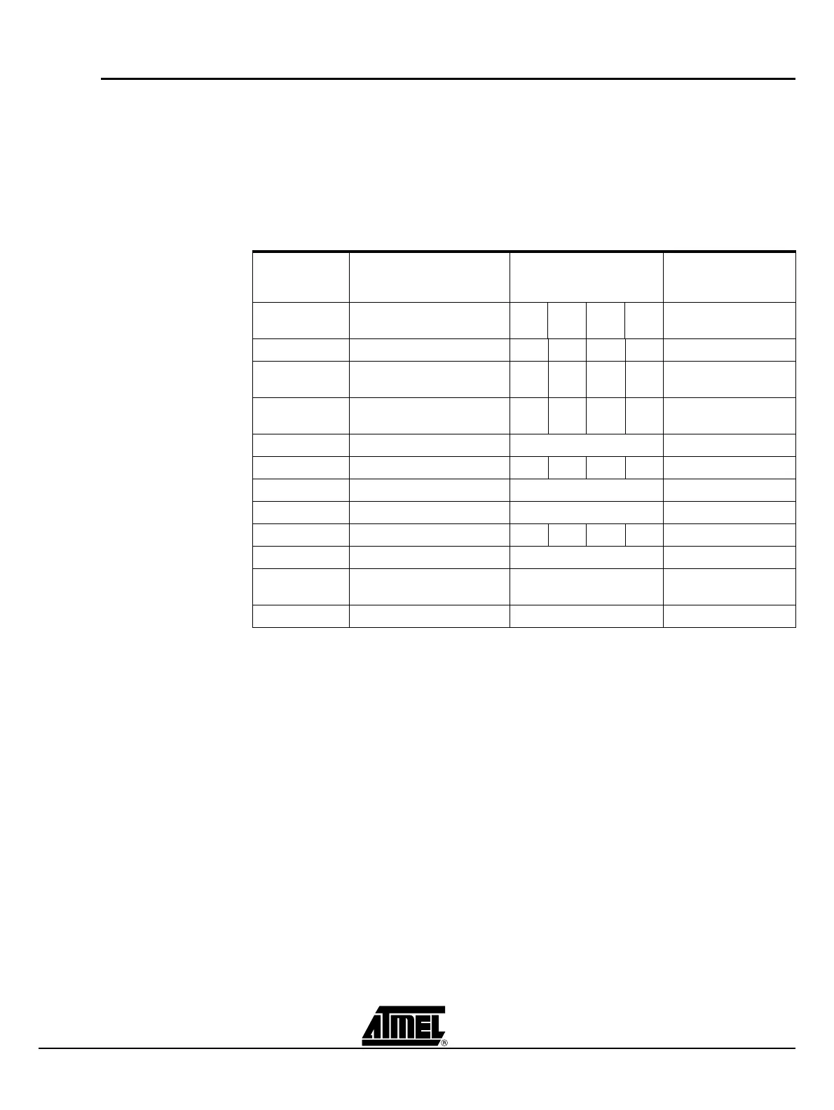
Table 1-2. A list of the Atmel 8051 Arithmetic Instructions.
Mnemonic Operation Addressing Modes
Execution Time in X1
Mode
@12 MHz (µs)
Dir Ind Reg
Im
m
ADD A, <byt>e A = A + <byte> X X X X
ADDC A,
<byte>
A = A + <byte> + C X X X X 1
SUBB A,
<byte>
A = A – <byte> – C X X X X 1
INC A A = A + 1 Accumulator only 1
INC <byte> <byte> = <byte> + 1 X X X 1
INC DPTR DPTR = DPTR + 1 Data Pointer only 2
DEC A A = A1 Accumulator only 1
DEC <byte> <byte> = <byte> – 1 X X X 1
MUL AB B:A = B × A ACC and B only 4
DIV AB
A = Int [A/B]
B = Mod [A/B]
ACC and B only 4
DA A Decimal Adjust Accumulator only 1
Question and Answer IconNeed help?

Do you have a question about the Atmel 8051 and is the answer not in the manual?

Atmel 8051 Specifications

General IconGeneral
Architecture8-bit
Serial CommunicationUART
CPU8051
Program MemoryUp to 64 KB Flash
Timers/Counters2 or 3 (16-bit)
SPIYes
I2CYes
ADCYes (some variants)
Operating Voltage2.7V to 5.5V
Operating Temperature-40°C to +85°C
PackageDIP, PLCC, TQFP

Summary

Section 1: The 8051 Instruction Set

1.1 Program Status Word

Details the Program Status Word (PSW) register, its bits, and their functions.

1.2 Addressing Modes

Describes the various addressing modes used by the 8051 instruction set.

1.3 Arithmetic Instructions

Lists and explains the arithmetic instructions available on the 8051.

1.4 Logical Instructions

Details the bitwise logical operations performed by the 8051 instruction set.

1.5 Data Transfers

Covers instructions for moving data between registers and memory.

1.6 External RAM

Details instructions for accessing external data memory.

1.7 Lookup Tables

Describes instructions for reading data from program memory tables.

1.8 Boolean Instructions

Covers the 8051's single-bit processor and its instructions.

1.9 Jump Instructions

Explains instructions that alter program flow, including jumps and calls.

1.10 Read-Modify Write Instruction Features

Explains instructions that read, modify, and write back data.

1.11 Instruction Set Summary

Provides a comprehensive list of 8051 instructions with byte and cycle counts.

1.12 Instructions That Affect Flag Settings

Lists instructions that modify the status flags in the PSW register.

1.13 Instruction Table

Presents a table of 8051 instructions with hex values and execution times.

1.14 Instruction Definitions

Provides detailed descriptions and operation of individual 8051 instructions.

Section 2: Common Features Description

2.1 Introduction

Introduces the chapter on on-chip hardware features of 8051 microcontrollers.

2.2 Special Function Registers

Details the Special Function Register (SFR) map and key registers.

2.3 Oscillator and Clock Circuit

Explains the on-chip oscillator and clock generation system.

2.4 CPU Timing

Details the CPU's fetch/execute cycles and timing characteristics.

2.5 Port Structures and Operation

Details the structure and operation of the 8051's I/O ports.

2.6 Accessing External Memory

Explains accessing external program and data memory via 8051 pins.

2.8 ALE

Explains the Address Latch Enable (ALE) signal for address multiplexing.

2.9 Timer/Counters

Introduces the two general-purpose 16-bit timers/counters in the 80C51.

2.10 Timer 0

Details the four operating modes of Timer 0.

2.11 Timer 1

Details Timer 1's operation, similar to Timer 0 but with mode 3 differences.

2.12 Timer 2

Details Timer 2 features: capture, auto-reload, and baud rate generation.

2.13 Serial Interface

Describes the Universal Asynchronous Receiver/Transmitter (UART) features.

2.14 Framing Error Detection

Explains the feature for detecting framing errors in asynchronous serial modes.

2.15 Automatic Address Recognition

Describes hardware feature for multiprocessor communication address matching.

2.16 Interrupts

Covers interrupt handling, priority levels, and response times.

Related product manuals