The 8051 Instruction Set
1-3 Atmel 8051 Microcontrollers Hardware Manual
4316B–8051–02/04
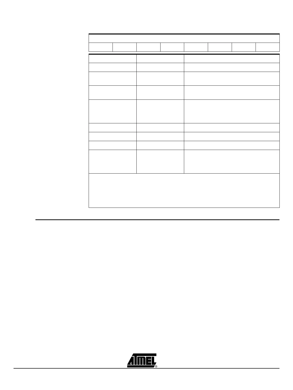
Table 1-1. PSW: Program Status Word Register
1.2 Addressing
Modes
The addressing modes in the 8051 instruction set are as follows:
1.2.1 Direct Addressing
In direct addressing the operand is specified by an 8-bit address field in the instruction.
Only 128 Lowest bytes of internal Data RAM and SFRs can be directly addressed.
1.2.2 Indirect Addressing
In indirect addressing the instruction specifies a register which contains the address of
the operand. Both internal and external RAM can be indirectly addressed.
The address register for 8-bit addresses can be R0 or R1 of the selected register bank,
or the Stack Pointer. The address register for 16-bit addresses can only be the 16-bit
“data pointer” register, DPTR.
1.2.3 Register Instructions
(MSB) (LSB)
CY AC F0 RS1 RS0 OV - P
Symbol Position Name and Significance
CY PSW.7 Carry flag
AC PSW.6
Auxiliary Carry flag.
(For BCD operations.)
F0 PSW.5
Flag 0
(Available to the user for general purposes.)
RS1 PSW.4
Register bank Select control bits 1 & 0. Set/cleared
by software to determine working register bank (see
Note).
RS0 PSW.3
OV PSW.2 Overflow flag.
- PSW.1 (reserved)
PPSW.0
Parity flag.
Set/cleared by hardware each instruction cycle to
indicate and odd/even number of “one” bits in the
accumulator, i.e., even parity.
Note:
The contents of (RS1, RS0) enable the working register banks as follows:
(0.0)-Bank 0(00H-07H)
(0.1)-Bank 1(08H-0FH)
(1.0)-Bank 2(10H-17H)
(1.1)-Bank 3(18H-1FH)