318
8271D–AVR–05/11
ATmega48A/PA/88A/PA/168A/PA/328/P
Notes: 1. “Max” means the highest value where the pin is guaranteed to be read as low
2. “Min.” means the lowest value where the pin is guaranteed to be read as high
3. Although each I/O port can source more than the test conditions (20mA at V
CC
= 5V, 10mA at V
CC
= 3V) under steady state
conditions (non-transient), the following must be observed:
ATmega48A/PA/88A/PA/168A/PA/328/P:
1] The sum of all I
OH
, for ports C0 - C5, D0- D4, ADC7, RESET should not exceed 150mA.
2] The sum of all I
OH
, for ports B0 - B5, D5 - D7, ADC6, XTAL1, XTAL2 should not exceed 150mA.
If II
OH
exceeds the test condition, V
OH
may exceed the related specification. Pins are not guaranteed to source current
greater than the listed test condition.
4. Although each I/O port can sink more than the test conditions (20 mA at V
CC
= 5V, 10 mA at V
CC
= 3V) under steady state
conditions (non-transient), the following must be observed:
ATmega48A/PA/88A/PA/168A/PA/328/P:
1] The sum of all I
OL
, for ports C0 - C5, ADC7, ADC6 should not exceed 100 mA.
2] The sum of all I
OL
, for ports B0 - B5, D5 - D7, XTAL1, XTAL2 should not exceed 100 mA.
3] The sum of all I
OL
, for ports D0 - D4, RESET should not exceed 100 mA.
If I
OL
exceeds the test condition, V
OL
may exceed the related specification. Pins are not guaranteed to sink current greater
than the listed test condition.
29.2.1 ATmega48A DC Characteristics
Notes: 1. Values with “Minimizing Power Consumption” enabled (0xFF).
R
RST
Reset Pull-up Resistor 30 60 kΩ
R
PU
I/O Pin Pull-up Resistor 20 50 kΩ
V
ACIO
Analog Comparator
Input Offset Voltage
V
CC
= 5V
V
in
= V
CC
/2
<10 40 mV
I
ACLK
Analog Comparator
Input Leakage Current
V
CC
= 5V
V
in
= V
CC
/2
-50 50 nA
t
ACID
Analog Comparator
Propagation Delay
V
CC
= 2.7V
V
CC
= 4.0V
750
500
ns
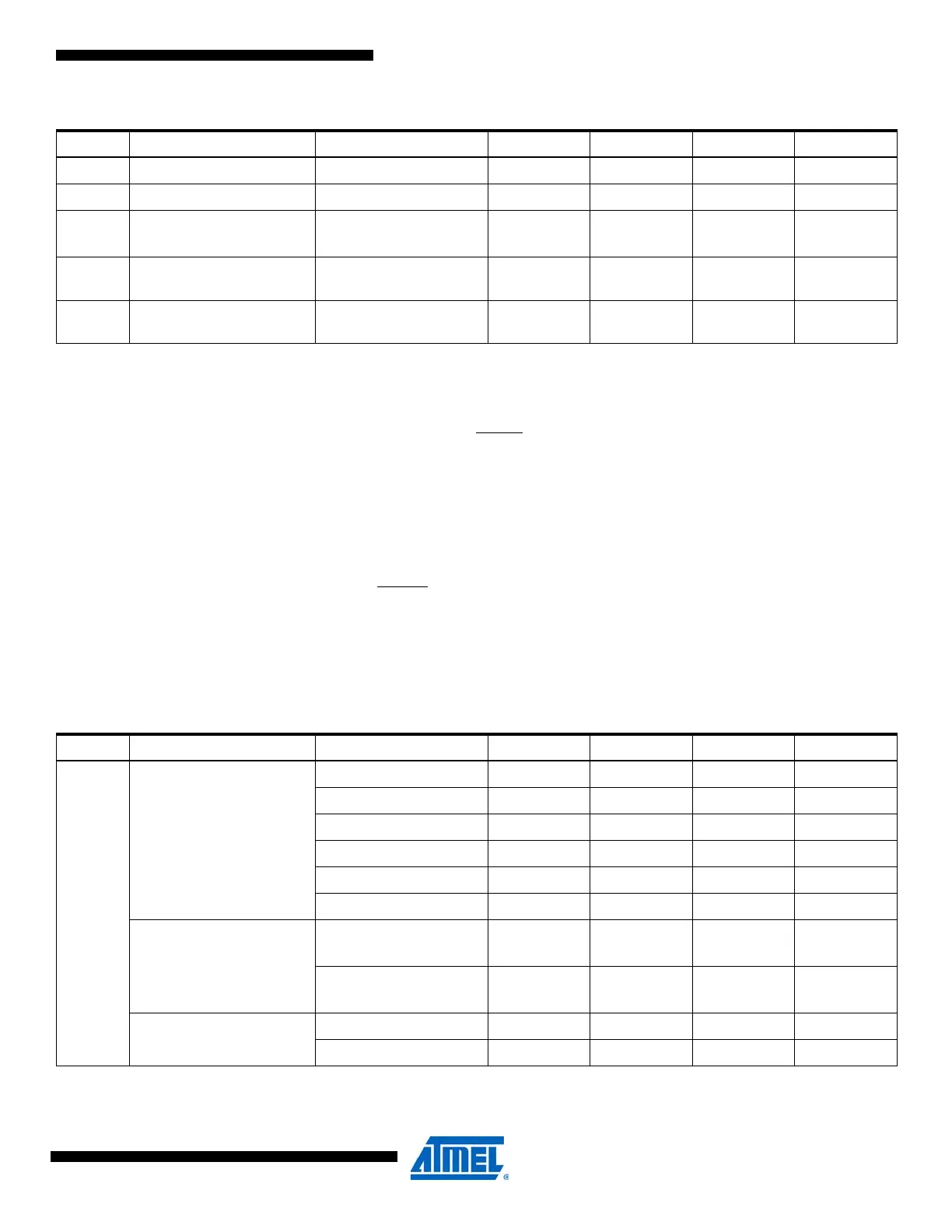
Table 29-1. Common DC characteristics T
A
= -40°C to 85°C, V
CC
= 1.8V to 5.5V (unless otherwise noted) (Continued)
Symbol Parameter Condition Min. Typ. Max. Units
Table 29-2. ATmega48A DC characteristics - T
A
= -40°C to 85°C, V
CC
= 1.8V to 5.5V (unless otherwise noted)
Symbol Parameter Condition Min. Typ.
(2)
Max. Units
I
CC
Power Supply Current
(1)
Active 1MHz, V
CC
= 2V 0.2 0.55 mA
Active 4MHz, V
CC
= 3V 1.2 3.5 mA
Active 8MHz, V
CC
= 5V 4.0 12 mA
Idle 1MHz, V
CC
= 2V 0.03 0.5 mA
Idle 4MHz, V
CC
= 3V 0.21 1.5 mA
Idle 8MHz, V
CC
= 5V 0.9 5.5 mA
Power-save mode
(3)
32kHz TOSC enabled,
V
CC
= 1.8V
0.75 µA
32kHz TOSC enabled,
V
CC
= 3V
0.9 µA
Power-down mode
(3)
WDT enabled, V
CC
= 3V 3.9 15 µA
WDT disabled, V
CC
= 3V 0.1 2 µA