94
8271D–AVR–05/11
ATmega48A/PA/88A/PA/168A/PA/328/P
14.4 Register Description
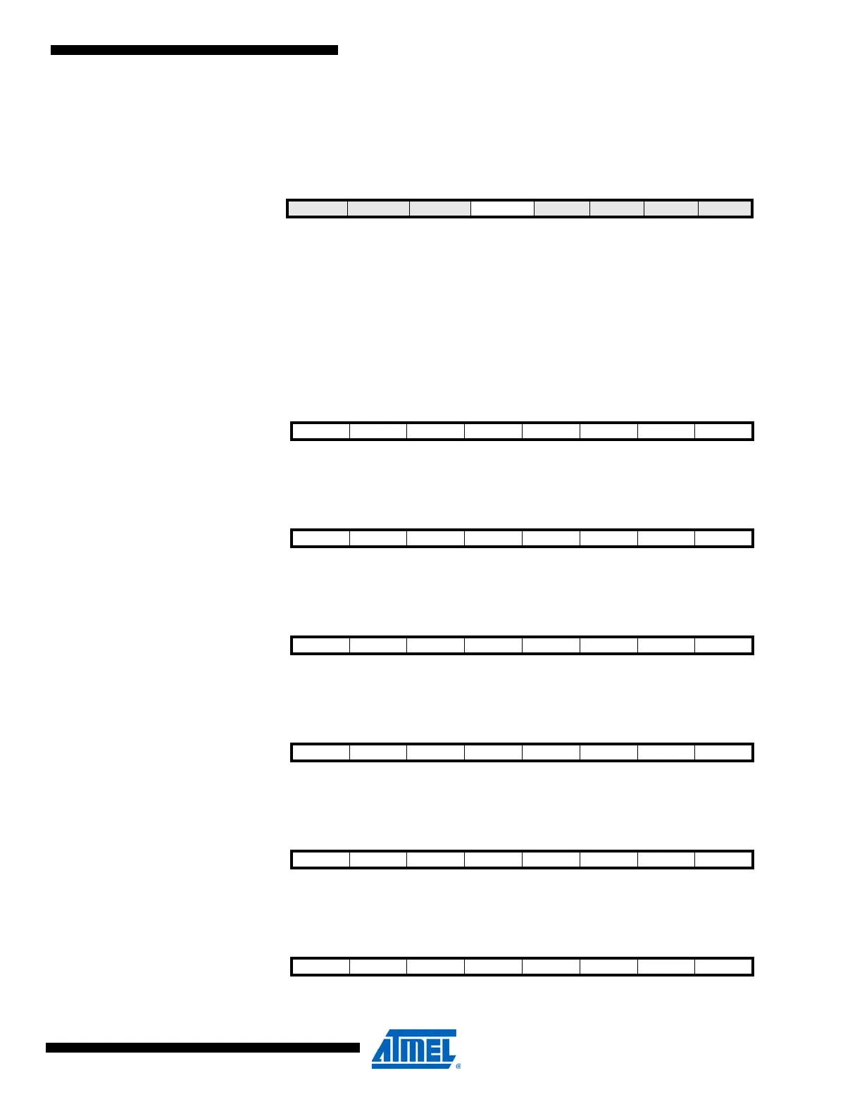
14.4.1 MCUCR – MCU Control Register
Notes: 1. BODS and BODSE only available for picoPower devices ATmega48PA/88PA/168PA/328P
• Bit 4 – PUD: Pull-up Disable
When this bit is written to one, the pull-ups in the I/O ports are disabled even if the DDxn and
PORTxn Registers are configured to enable the pull-ups ({DDxn, PORTxn} = 0b01). See ”Con-
figuring the Pin” on page 78 for more details about this feature.
14.4.2 PORTB – The Port B Data Register
14.4.3 DDRB – The Port B Data Direction Register
14.4.4 PINB – The Port B Input Pins Address
(1)
14.4.5 PORTC – The Port C Data Register
14.4.6 DDRC – The Port C Data Direction Register
14.4.7 PINC – The Port C Input Pins Address
(1)
Bit 7 6 5 4 3 2 1 0
0x35 (0x55)
– BODS
(1)
BODSE
(1)
PUD – – IVSEL IVCE MCUCR
Read/Write R R/W R/W R/W R R R/W R/W
Initial Value 0 0 0 0 0 0 0 0
Bit 76543210
0x05 (0x25)
PORTB7 PORTB6 PORTB5 PORTB4 PORTB3 PORTB2 PORTB1 PORTB0 PORTB
Read/Write R/W R/W R/W R/W R/W R/W R/W R/W
Initial Value 0 0 0 0 0 0 0 0
Bit 76543210
0x04 (0x24) DDB7 DDB6 DDB5 DDB4 DDB3 DDB2 DDB1 DDB0 DDRB
Read/Write R/W R/W R/W R/W R/W R/W R/W R/W
Initial Value 0 0 0 0 0 0 0 0
Bit 76543210
0x03 (0x23) PINB7 PINB6 PINB5 PINB4 PINB3 PINB2 PINB1 PINB0 PINB
Read/Write R/W R/W R/W R/W R/W R/W R/W R/W
Initial Value N/A N/A N/A N/A N/A N/A N/A N/A
Bit 76543210
0x08 (0x28)
– PORTC6 PORTC5 PORTC4 PORTC3 PORTC2 PORTC1 PORTC0 PORTC
Read/Write R R/W R/W R/W R/W R/W R/W R/W
Initial Value 0 0 0 0 0 0 0 0
Bit 76543210
0x07 (0x27) – DDC6 DDC5 DDC4 DDC3 DDC2 DDC1 DDC0 DDRC
Read/Write R R/W R/W R/W R/W R/W R/W R/W
Initial Value 0 0 0 0 0 0 0 0
Bit 76543210
0x06 (0x26) – PINC6 PINC5 PINC4 PINC3 PINC2 PINC1 PINC0 PINC
Read/Write R R/W R/W R/W R/W R/W R/W R/W
Initial Value 0 N/A N/A N/A N/A N/A N/A N/A