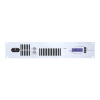
BW Broadcast technical manual
Page 35
Technical data
3.23 POWER AMPLIFIER BOARD
The RF signal from the exciter section of the combo board arrives at the MCX RF input connector CON1 via a
coaxial cable. From here the 50 ohm input impedance is matched to the gate of the FET transistor T1 by the
impedance matching network formed by C1, C2, C34, L1 and L9. R1, R2, VR2 and C3 provide bias control to the
gate of T1 from the output of REG1 which is a 18 volt regulator derived from the 24 Volt line of the AUX power
supply module. C6 and C7 provide decoupling for the regulator. L4, C5, R3 and L3 provide 24 volts to T1’s drain
from the 24 volt AUX line as well as providing some impedance matching to the output of T1. Further impedance
matching from T1’s drain is composed of C4, L2 and VC1 and RFT1. RFT1 is a four to one balun that provides an
unbalanced to balanced connection to the two Gates of gemini packaged FET transistor T2. Both gates of T2 are
each biased with 2 parralled 12 Ohm resistors.
The drain outputs of T2 are connected to another balun transformer RFT2 which provides four to one impedance
step up as well as proving a DC feed to the transistors drains via a center tapped winding. The DC power applied
to the center of RFT2 comes from the main adjustable power supply module which can control the RF power out-
put by having it’s output voltage adjusted over a 12 to 35 volt range. C8-14, L5, and R9 provide filtering and RF
decoupling to the power feed into the center tap RFT2.
The RF output side of the balun is fed into a low pass filter composed of C15-21 and inductors L6 to L8. These
components reduce the level of any harmonic products generated by the power amplifier. The output of the low
pass filter feeds into the VSWR sensor which generates our forward and reverse RF power measurements for
metering and for VSWR fault protection and alarms. The RF line passes through ferrite ring RFT3. This ring also
has 14 turns of wire as a secondary winding. IC1 and associated resistors R13-R26 buffer the sensors outputs
and provide a level suitable for the control/LCD boards microcontroller and protection circuitry.
The RF output sniff for the front panel is realized by R34 which is placed very close to the RF output line. A coaxi-
al cable connects this picked up RF output to the front panel.
A temperature sensor circuit is located close to the main RF transistor T2. This temperature sensor is mounted
into the heatsink and consists of the sensor itself TS1 which is located under the board and an op-amp circuit
for level adjustment. The op-amp IC2 and associated components R10 and R27-R32 convert the output signal
from the sensor itself to a level more suitable for the microcontroller and protection circuitry on the Control / LCD
board.
CON2 connection block provides an interface to the board for the power connections from the two power supply
modules. CON5 provides an interface to the LCD control board. This connector carrys readings for the forward
and reverse power, temperature, PA voltage, 18 volts from the regulator off the AUX power line to power the
LCD control board and the combo board, and last but not least the PA power modules control line which controls
it’s output voltage. This control signal is derived from the LCD / control board and is wired through the power
amplifier PCB and out through CON2 to the power supply module.