The volume control and balance relays are driven from three 8-bit serial-in parallel-out (SIPO) shift
registers on the front panel PCB. The logic signals come in on CN6, CN8 and CN9, and control the 7-
way open-collector relay drivers U4,U5,U7. Driver U7 also controls the mains on/o and inrush relays,
(on the PSU PCB) the two amplier output relays, (on the right amplier PCB).
R111 is a pull-up resistor which allows MAINS ON/OFF RELAY to go high during testing if the PSU
board is not being used to power front-panel and preamp PCBs, and thus permits the LED control to
work properly in this condition.
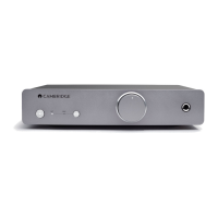
Headphone socket
The phones Left and Right signals come in from the two amplier PCBs. When a jack is inserted in to
the phones socket, the normally-closed contacts open, and the PHONES DETECT signal goes low,
signalling the PIC to open the output relays and disconnect the loudspeakers.
Power Amplier PCBs
The power amplier boards are very similar. The left channel is described in detail, and the right channel
description deals only with the dierences.
Power Amplier Left PCB
This description is subdivided as follows:
Input stage
DC trim system.
The Voltage Amplier Stage
Biasing system
Output stage
The XD Crossover Displacement system
Power supplies
Overload protection
Clip detection
DC oset protection
Over-temperature protection
Speaker short-circuit detection
Headphone output attenuator
DC trim system.
VR2 and its associated components make up the DC trimming network; this allows to output DC oset
to be reduced to less than 1mV.
The XD Crossover Displacement system.
The essence of the Crossover Displacement principle is the injection of an extra current, varying with
the signal, into the output point of a conventional Class-B output stage, with the result that the
crossover point is displaced away from the no-signal voltage. The displacement current is made
proportional to the output voltage. For example, if the displacement current is 1 Amp with the output
at quiescent at 0V, it is set to increase to 2 Amps with the output fully negative, and to reduce to zero
with the output fully positive.
55
 Loading...