Do you have a question about the Cambridge Audio 840A and is the answer not in the manual?
Details the amplifier's power output in Ohms.
Specifies total harmonic distortion at 80% of rated power.
Lists the frequency range and deviation.
Indicates the signal-to-noise ratio.
Details impedance for different inputs.
Specifies the damping factor.
Indicates maximum power draw.
Specifies power draw when idle or in standby.
Describes the type and range of tone controls.
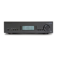
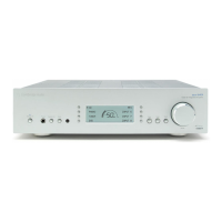
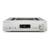
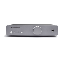
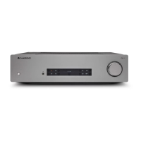
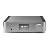
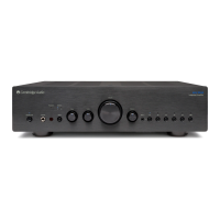
Provides the physical dimensions of the unit.
States the product's weight.
Covers warnings for electrical shock, servicing, and component handling.
Provides guidance on replacing components like tantalum capacitors.
Illustrates the overall signal flow and component connections.
Visual representation of product components.
Detailed list of components shown in the exploded diagram.
Circuit diagrams for microcontroller, LCD, and shift registers.
Physical layouts of the top and bottom sides.
Bill of Materials for the front panel PCB.
Circuit diagrams for input selection, control, and amplifier.
Physical layouts of the top and bottom sides.
Bill of Materials for the input PCB.
Circuit diagrams for relay logic, tone control, and post amp.
Physical layouts of the top and bottom sides.
Bill of Materials for the preamp PCB.
Circuit diagrams for power supplies and right channel.
Physical layouts of the top and bottom sides.
Bill of Materials for the right power amp PCB.
Circuit diagrams for the left channel amplifier and power supplies.
Physical layouts of the top and bottom sides.
Bill of Materials for the left power amp PCB.
Circuit diagram for the Hub PCB.
Physical layouts of the top and bottom panels.
Bill of Materials for the Hub board.
Circuit diagram for the Rectifier PCB.
Physical layouts of the top and bottom sides.
Bill of Materials for the Rectifier PCB.
Pinouts for frequently used integrated circuits.
Pinouts for PIC and ULN2003A devices.
Details the functions and components of the Power Supply PCB.
Details the main PIC, controls, and interfaces.
Outlines the functions of the Input PCB.
Lists components and functions of the Preamp PCB.
Describes amplifier stages, protection, and ancillary functions.
Describes the functions of the Hub board and its microcontroller.
Explains the components and purpose of the Rectifier PCB.
Step-by-step guide to load software onto the amplifier.
Instructions for loading the firmware file and downloading code.
| Frequency Response | 10Hz - 50kHz ±1dB |
|---|---|
| Input Impedance | 47k Ohms |
| Power Output | 120W per channel into 8 Ohms |
| Total Harmonic Distortion | <0.001% (1kHz, 80% of rated power) |
| Dimensions | 115 x 430 x 385 mm (4.5 x 16.9 x 15.2 inches) |
| Damping Factor | >100 |
| Signal to Noise Ratio | >93dB (unweighted) |