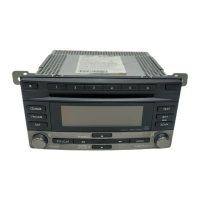
ADJUSTMENT OF ZR1/PF3 DSP TUNER: 880-2091E
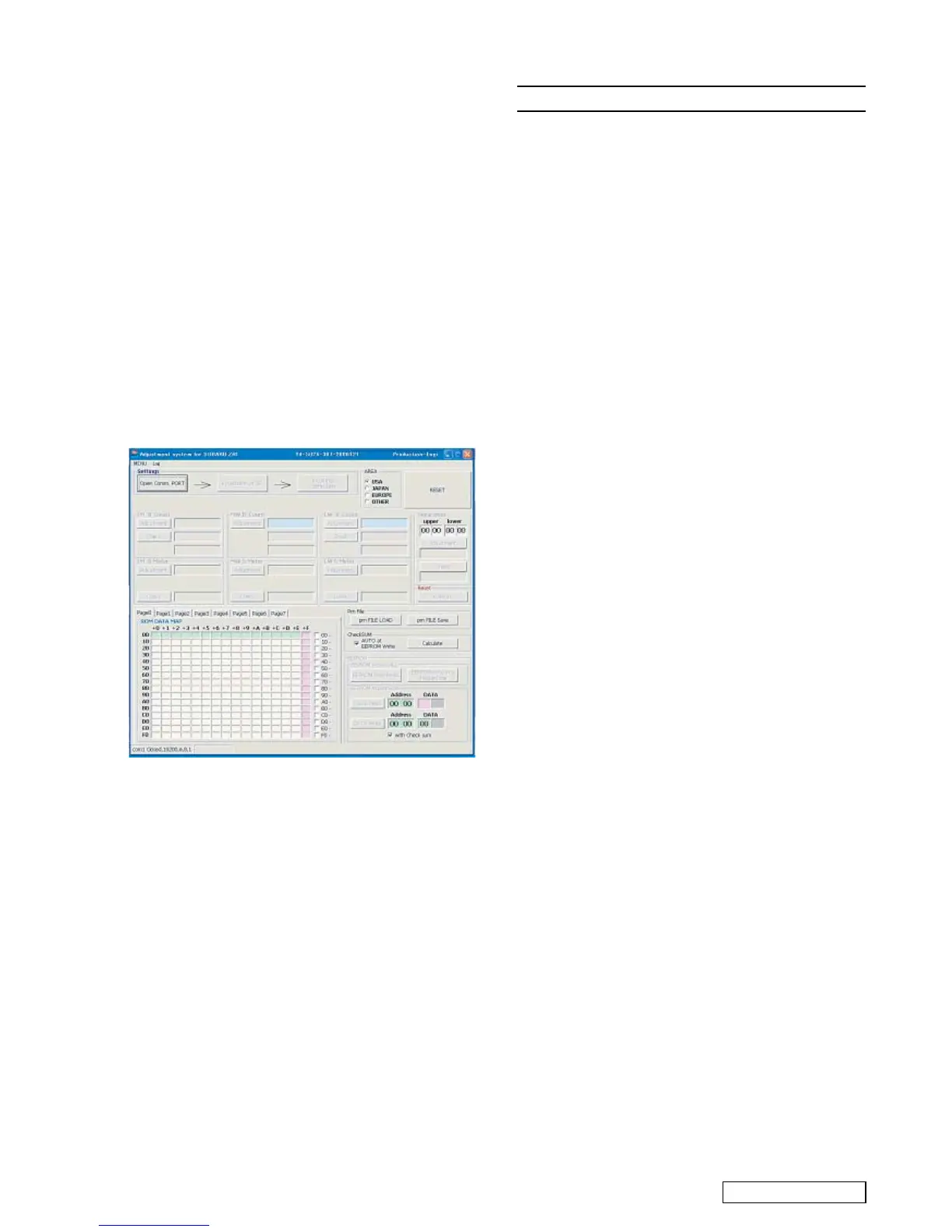
Setting
1 Open 2 switches of MICOM(EEP-ROM).
2 Open the Adjustment software:SUBARU_ZR1_ADJ_DSP_V307.exe
and turn on the unit.
3 Select “EUROPE” in the “AREA” box. Click the “Settings” items
in the following order:
Open Comm.PORT->Initialization of JIG->Incoming connection.
4 After 2 minutes, set the following items.
FM Adjustments
1 FM IF-Count
1-1 Set the reception frequency to 98.1MHz
1-2 Set the SG output to 60dBu.
1-3 Click “Adjustment”
2 FM S-Meter
2-1 Set the reception frequency to 98.1MHz
2-2 Set the MONO to 1kHz/22.5kHz variable.
2-3 Set the SG output to 20dBu.
2-4 Click “Adjustment”
AM Adjustments
1 MW/LW IF-Count
1-1 Use the AM ANT DUMMY.
1-2 Set the reception frequency to 1000kHz
1-3 Set the SG output to 60dBu.
1-4 Click “Adjustment”
2 MW/LW S-Meter
2-1 Use the AM ANT DUMMY.
2-2 Set the reception frequency to 1000kHz
2-3 Set the MONO to 400Hz/30% variable.
2-4 Set the SG output to 40dBu.
2-5 Click “Adjustment”
Writing data
1 Click “EEPROM Page Read”, and then “ROM DATA MAP” displays.
2 Input “00” into the right box of the “ROM DATA MAP”.
3 Select the “AUTO at EEPROM Write” of the “CheckSUM”. Then
click “ Calculate”.
4 Click “EEPROM Write in a checked line”, and then the data is
written in EEPROM-IC.
ADJUSTMENTS
052-3214-80 M30876FJAGP System Controller
Terminal Description
EXPLANATION OF IC
PF-2945A-A/PF-2982B-A
-3-
Illumination control signal input.
pin 2
5V Power supply ON signal output. H = ON.
pin 3
8V Power supply ON signal output. H = ON.
pin 6
Data length selection(8bit/16bit).
pin 7
Strong electric field d etection signal input.
pin 10
Reset signal input.
pin 11
Crystal connection.
pin 12
Crystal connection.
pin 14
Positive voltage supply.
pin 15
Nonmaskable interrupt. Connect to VDD via
aresistor.
pin 16
ACC detection signal input.
pin 17
Backup detection signal input.
pin 18
RDS/RBDserialclockinput.
pin 19
RDS/RBD serial data input.
pin 20
Muting signal output to the Audio power
amplifier.
pin 21
Serial data input from the CAN IC.
pin 22
Serial data output to the CAN IC.
pin 23
Error signal input from the CAN IC.
pin 24
Audio power amplifier ON signal output.
pin 25
MP3/GIX request signal input.
pin 26
DSP/EEP serial clock output.
pin 28
DSP/EEP serial data output.
pin 29
Flash memory Serial data output.
pin 30
Flash memory Serial data input.
pin 31
Antenna ON command output.
pin 32
The fan on signal output.
pin 33
MP3/6CD-mechanism serial data output.
pin 34
MP3/6CD-mechanism serial clock output.
pin 35
MP3/6CD-mechanism reset pulse output.
pin 36
MP3 standby/6CD-mechanism system ACC
control.
pin 37
MP3 S-RAM standby signal output.
pin 38
DSP automatic mute control. L = mute on.
pin 39
Tuner mute signal output.
pin 40
Initial signal input from the DSP IC.
pin 43
Reset signal output to the DSP IC.
pin 44
VFD ON signal output.
pin 45
Illumination ON signal input.
pin 46
Reset pulse output to the DAC. L = reset.
pin 47
8V Power supply ON signal output. H = ON.
pin 48
3.3V Power supply ON signal output. H = ON.
pin 49
1.5V Power supply ON signal output. H = ON.
pin 50
CD-BUS in/out. EQ data output.
pin 51
CD-BUS in/out. EQ clock output.
pin 52
CD-BUS in/out. Input the activating signal
to change the soft.
pin 53
CD IC clock pulse output.
pin 55
Chip enable signal output to the CD IC.
pin 56
Reset pulse output to the CD IC.
pin 57
At loading, detects the chucking. And next,
detects the inside limit of the pick up position.
pin 58
CD disk chucking signal input for the CD
mechanism.
pin 59
Photo sensor signal input from the CD
mechanism.
pin 60
Photo sensor signal input from the CD
mechanism.
 Loading...