5
5
4
4
3
3
2
2
1
1
D D
C C
B B
A A
PS8625 (eDP to LVDS)
PWMI: 0~100KHz, 0~100% duty cycle
Single link
LVDS
single PCB trace
I2C_ADDR: I2C Slave address selection, internal pull-down ~80K
L: 0x10h~0x1Fh
H: 0x90h~0x9Fh
RLV_CFG: LVDS color depth and data mapping selection, internal pull-down ~80K
L: 8-bit LVDS, VESA mapping
M: 8-bit LVDS, JEIDA mapping
H: 6-bit LVDS, both VESA and JEIDA mapping
Power On Configuration
RLV_LNK: LVDS single link or dual link selection, internal pull-down ~80K
L: Single link LVDS
H: Dual link LVDS
ᓮ
ᓮᓮ
ᓮᒔ
ᒔᒔ
ᒔᎁ
ᎁᎁ
ᎁ
PANEL SPEC
ᓳ
ᓳᓳ
ᓳᖞ
ᖞᖞ
ᖞ
(Even)
Dual link
LVDS
PIN13/14
6-19-41001-019
6-19-31001-247
PIN38PIN50 PIN6 PIN6 PIN6
eDP
LVDS
LVDS
eDP
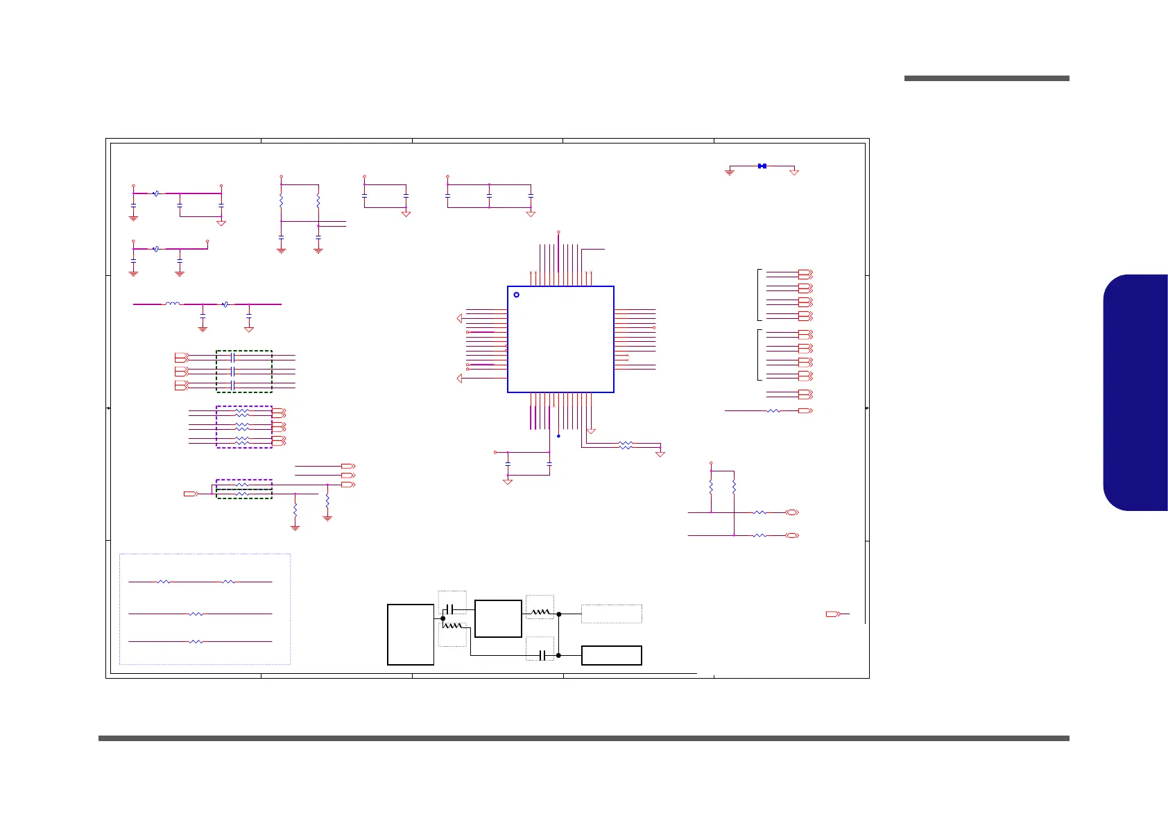
1. Place the switching regulator inductor (L3) close to SW_OUT Pins (Pin15, Pin16).
2. The SW_OUT output traces should be as wide as possible.
3. The GNDX pins (Pin17, Pin18) should be connected to the main PCB ground plane, with the device GND pins of the PS8625 connected to separate GND island (GNDA) for the
device.
The GND island (GNDA) should be connected to the main GND plane (GND) with a single-point connection by use of a wide PCB trace.
4. Place the 4.7uF decoupling Capacitor (C4) for VDDIOX close to VDDIOX pin.
5. The GND of the 4.7uF capacitor (C4) for VDDIOX should be placed close to the GND of 4.7uF capacitor (C5) behind Inductor.
6. Place the bead (L2) for VDDIOX close to PS8625.
Switching Regulator Layout Guideline
Note:
The decoupling caps C24, C28, C31, C26, C37, C38
shall be close to the power pins as possible
/9'6
Ղ
ՂՂ
Ղٙ
ٙٙ
ٙ
/9'6
Ղ
ՂՂ
Ղٙ
ٙٙ
ٙ
H'3
Ղ
ՂՂ
Ղٙ
ٙٙ
ٙ
H'3
Ղ
ՂՂ
Ղٙ
ٙٙ
ٙ
('3&RQQ3DQHO
pin17,19
+DVZHOO
36
pin7,9
/9'6&RQQ3DQHO
PS8625_12A
6-03-08625-031
LVDS-U0N
LVDS-U0P
LVDS-U1N
LVDS-U1P
LVDS-U2P
LVDS-UCLKP
LVDS-UCLKN
LVDS-U2N
P_DDC_CLK
P_DDC_DATA
LVDS-L0N
LVDS-L0P
LVDS-L1N
LVDS-L1P
LVDS-L2N
LVDS-L2P
LVDS-LCLKN
LVDS-LCLKP
GND_PS8625
RLV_LNK VDDIO
VDDIO
RLV_CFGGND
LVDS_PLVDD_EN
VDDIO
PANEL_PWM
SW_OUT
RST#
PS8625_PD#
EDP_TXP_0
DAUXn
DAUXp
DRX0p
DRX0n
DRX1p
EDP_AUXN
EDP_AUXP
DRX1n
EDP_TXN_0
EDP_TXP_1
EDP_TXN_1
EDP_AUXP
EDP_AUXN
EDP_TXP_0
EDP_TXN_0
EDP_TXP_1
EDP_TXN_1
PWM_IN
RLV_CFG
LVDS-L0P
CSDA/MSDA
LVDS-L1N
RLV_LNK
DRX0n
LVDS-L1P
DRX0p
DAUXn
DRX1n
CSCL/MSCL
LVDS-L2N
LVDS-U0N
LVDS-U2P
DAUXp
VDDIOX
SW_OUT
LVDS-U0P
RST#
GND_PS8625
VDDIOX P_DDC_CLK
LVDS-LCLKP
LVDS-UCLKP
LVDS_PLVDD_EN
LVDS-UCLKN
GND_PS8625
SW_OUT
LVDS-U1N
PS8625_REXT
PS8625_PD#
LVDS-L2P
GND
LVDS-U1P
ENBLT
PANEL_PWM
LVDS-LCLKN
P_DDC_DATA
GND
LVDS-U2N
LVDS-L0N
GND_PS8625
VDD12
DRX1p
PWM_IN
RLV_AMP
HPD
HPD
ENBLT
LVDS_PLVDD_EN
VDD12 VDDRX
CSCL/MSCL
CSDA/MSDA
GND_PS8625
GND_PS8625
GND_PS8625
GND_PS8625
GND_PS8625
3.3VS
3.3VS
VDDIO
VDDIO
VDDIO VDDRX
VDDIOX
GND_PS8625
GND_PS8625
GND_PS8625
GND_PS8625
GND_PS8625
VDDIO
VDDIO
VDDIOX
VDD12
VDDRX
VDDIOX
3.3VS
LVDS-U1P 11
LVDS-U2N 11
LVDS-U2P 11
LVDS-UCLKN 11
LVDS-UCLKP 11
LVDS-U0N 11
LVDS-U0P 11
LVDS-U1N 11
P_DDC_CLK 11
P_DDC_DATA 11
LVDS-L2P 11
LVDS-LCLKN 11
LVDS-LCLKP 11
LVDS-L0N 11
LVDS-L0P 11
LVDS-L1N 11
LVDS-L1P 11
LVDS-L2N 11
DP_AUX# 11
DP_AUX 11
DP_TXP0 11
DP_TXN0 11
DP_TXP1 11
DP_TXN1 11
PANEL_PWM 11
EDP_BRIGHTNESS24
EDP_AUXP2
EDP_TXN_02
EDP_TXP_12
EDP_TXN_12
EDP_TXP_02
EDP_AUXN2
3.3VS8,9,11,12,13,22,24,25,26,27,28,29,31,32,33,34,35,36,37,38,41,46,48
EDP_HPD 11,26
ENBLT 11,33
LVDS_PLVDD_EN 11
SMC_VGA_THERM 20,33
SMD_VGA_THERM 20,33
Title
Size Document Number Rev
Date: Sheet
of
6-71-N5500-D02A
D01
[10] PS8625 (eDP to LVDS)
A3
10 55Wednesday, September 09, 2015
ᙔ!Ϻ!ႝ!တ!!DMFWP!DP/
N550RC
Title
Size Document Number Rev
Date: Sheet
of
6-71-N5500-D02A
D01
[10] PS8625 (eDP to LVDS)
A3
10 55Wednesday, September 09, 2015
ᙔ!Ϻ!ႝ!တ!!DMFWP!DP/
N550RC
Title
Size Document Number Rev
Date: Sheet
of
6-71-N5500-D02A
D01
[10] PS8625 (eDP to LVDS)
A3
10 55Wednesday, September 09, 2015
ᙔ!Ϻ!ႝ!တ!!DMFWP!DP/
N550RC
ER6 0_04
ER7 0_04
VC7
0.01u_50V_X7R_04
VR3 0_04
VL4
BCNR3010C-2R2M
VC21
0.01u_50V_X7R_04
VC6
0.1u_10V_X7R_04
R120
100K_04
VR23
10K_04
VR27
*4.7K_04
VR7 4.7K_04
VC1
0.47u_10V_Y5V_04
ER1 0_04
VR6 4.99K_1%_04
ER9 0_04
VC17
2.2u_6.3V_X5R_04
VR5 *4.7K_04
VC18
4.7u_6.3V_X5R_06
VL1
HCB1005KF-121T20
VR9 4.99K_1%_04
ER8 0_04
VC19
1u_6.3V_X5R_04
VC9
1u_6.3V_X5R_04
VC20
0.47u_10V_Y5V_04
VR26
*4.7K_04
VR1
100K_04
VR22
10K_04
VC15 0.1u_10V_X7R_04
VC3
1u_6.3V_X5R_04
VC2
0.1u_10V_X7R_04
VC16 0.1u_10V_X7R_04
ER11 0_04
VL2
HCB1005KF-121T20
VR24 0_04
VC12 0.1u_10V_X7R_04
VR10 1K_04
VR25 0_04
ER10 0_04
VC14 0.1u_10V_X7R_04
VC5
0.1u_10V_X7R_04
VR8 *4.7K_04
VL3
HCB1005KF-121T20
VC13 0.1u_10V_X7R_04
VC8
4.7u_6.3V_X5R_06
VU1
PS8625_12A
SW_OUT
15
SW_OUT
16
GNDX
17
GNDX
18
VDD12
19
TESTMODE
20
RLV_LNK/GPIO0
21
RLV_CFG
22
ENBLT
23
CSDA/MSDA
24
CSCL/MSCL
25
REXT
26
BLV_AMP
27
GND
28
TA1n
42
TA1p
41
TB1n
40
TB1p
39
VDDIO
38
TC1n
37
TC1p
36
TCK1n
35
TCK1p
34
ENPVCC/I2C_ADDR
33
TD1n
32
TD1p
31
DDC_SDA
30
DDC_SCL
29
NC
56
NC
55
TA0n
54
TA0p
53
TB0n
52
TB0p
51
VDDIO
50
TC0n
49
TC0p
48
TCK0n
47
TCK0p
46
PWMI
45
TD0n
44
TD0p
43
DAUXn
1
DAUXp
2
GND
3
DRX0p
4
DRX0n
5
VDDRX
6
DRX1p
7
DRX1n
8
RST#
9
PD#
10
HPD
11
PWMO
12
VDDIOX
13
VDDIOX
14
Epad
57
VR11 *4.7K_04
VC11 0.1u_10V_X7R_04
VC10
4.7u_6.3V_X5R_06
VC22
0.1u_10V_X7R_04
VC4
22u_6.3V_X5R_08
VR4
*20mil_short_04