Schematic Diagrams
B - 1
B.Schematic Diagrams
Appendix B: Schematic Diagrams
Table B - 1
SCHEMATIC
DIAGRAMS
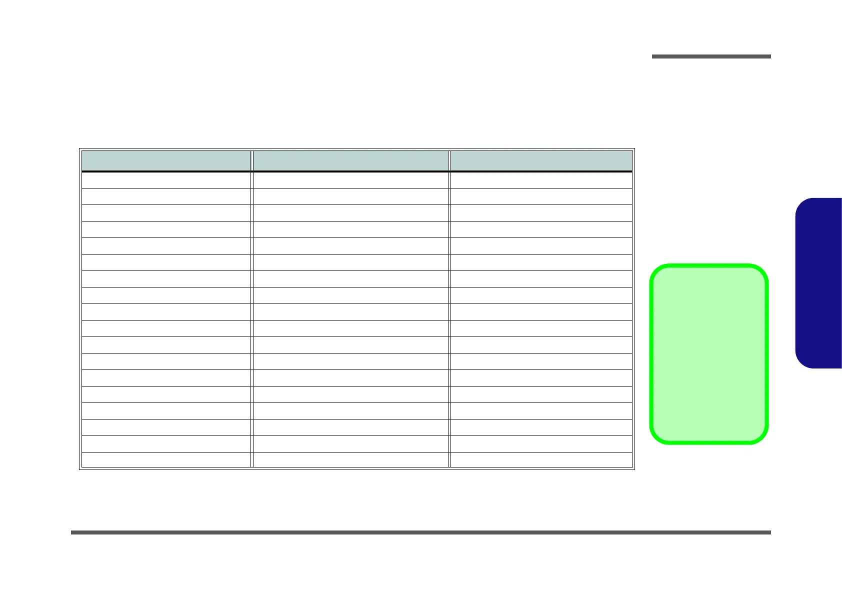
This appendix has circuit diagrams of the NJ50PU / NJ51PU notebook’s PCB’s. The following table indicates where to
find the appropriate schematic diagram.
Diagram - Page Diagram - Page Diagram - Page
System Block Diagram - Page B - 2 DP to VGA IT6516 - Page B - 20 MP2964 Controller - Page B - 38
Processor 1/13 - Page B - 3 RGB KB - Page B - 21 VCore - Page B - 39
Processor 2/13 - Page B - 4 TPM, PW Button, LID SW, LED - Page B - 22 VCCGT - Page B - 40
Processor 3/13 - Page B - 5 Type-C - Page B - 23 VCCIN - Page B - 41
Processor 4/13 - Page B - 6 PD Controller IT8851 - Page B - 24 Charger - Page B - 42
Processor 5/13 - Page B - 7 M Key PCIE SSD - Page B - 25 AC IN - Page B - 43
Processor 6/13 - Page B - 8 USB, HDD, ODD - Page B - 26 Audio Board - Page B - 44
Processor 7/13 - Page B - 9 LAN I219V - Page B - 27 Audio Board - Page B - 45
Processor 8/13 - Page B - 10 Card Reader OZ711 - Page B - 28 Click Board - Page B - 46
Processor 9/13 - Page B - 11 M.2 Card (3G/LTE) - Page B - 29 ODD to HDD Caddy - Page B - 47
Processor 10/13 - Page B - 12 M.2 Card (BT/WLAN) - Page B - 30 LID SW Board - Page B - 48
Processor 11/13 - Page B - 13 Audio Codec - Page B - 31 Power Seq. - Page B - 49
Processor 12/13 - Page B - 14 CONN FAN, TP, CCD, LED - Page B - 32
Processor 13/13 - Page B - 15 KBC ITE IT5570 - Page B - 33
DDR4 SO_DIMM_A - Page B - 16 VDD3 / VDD5 - Page B - 34
DDR4 SO_DIMM_B - Page B - 17 3.3V, 5V, 3VS, 5VS, CTL - Page B - 35
Panel, Inverter - Page B - 18 2.5V, VCCST, VCCSTG - Page B - 36
HDMI - Page B - 19 VDDQ, VDDQ_VTT, 1.8VA - Page B - 37
Version Note
The schematic dia-
grams in this chapter
are based upon version
6--7P-NJ5P5-002. If
your mainboard (or oth-
er boards) are a later
version, please check
with the Service Center
for updated diagrams
(if required).