condition based
on the
power being
delívered
for
the
existing heat
level.
The
ODER
amplifier accepts
íhis
input
informaíion
and, using
an RC
modei
of the
heat transfer
characteristics
of the
output
devíces
(as
mounted
in the
heatsinks), creates
a
complex output
proportional
to
thermal reserve.
Output
from
the
positive
ODER
amplifier ranges
from
-12V
(cold)
to +9V
(hard
ODER).
This output drives
the
positive
Low
Síde
bias feed control
circuit
and the
negative High Side Voltage Translator feed control
circuit.
Also,
this circuit provides test
poini
moniíoring information
and
Bi-ODEP
VZ
mode
control information.
Output from
the
negative
ODER
amplifier ranges from
+12V
(cold)
to -
9V
(hard
ODER).
This output drives
the
negative
LS
bias feed control
circuit
and the
positive
HS
Voltage Translator feed control circuit. Also,
this circuit provides test point monitoring information, Bi-ODEP
VZ
mode
control information,
and
front panel
ODER
(thermal reserve)
LED
control information.
Channel
1
ODER
Circuitry
shown
(channel
2 is
idéntica!)
Notes
ODER
Inputs:
Temperatura
±VCC
Output
Current
OffMain
Module
oo—
LM-334Z
nermal
Sensor
2.98Vat25'C,
lOmV/'CRise)
CC
•s
Q519
LS
Output
$Re
I
Dutput
Buss
I
I
?Re
/
Q524
LS
•>
Output
*J
CC
CC^
LM-334Z
hermal
Sensor
+Ten
+VC
+IC
+ICC
-ICO
-1C1
-VC
-Ten
p1
M1
M1
p1
ODER
Outputs:
Calibrated Temperature,
for
monitoring
±ODEP Level,
for
monitoring
±ODEP Level,
for
Bi-ODEP control
of VZ
Supply
±ODEP Level,
to
limit drive
at
±Voltage Transiators (±LH)
±ODEP Level,
to
limit
Low
Side Bias (±LL)
ODER
Indication
(front
panel LEDs)
On
Main Module
Hot
-+9V
Calibrated
Temperatura
Output
Buffer
Amplifier
Thermal
Limit
Amplifier
-12V
*+ODEP
Output
-LH1
+LL1
FAULT1
PWR1
PWR
LOSS
+LH1
-LL1
*--ODER
Output
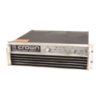
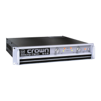
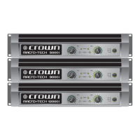
MA-5000VZ-13
 Loading...