Document No. 002-14949 Rev. *E Page 63 of 113
12.3.1 Multiplexed Bluetooth GPIO Signals
The Bluetooth GPIO pins (BT_GPIO_0 to BT_GPIO_7) are multiplexed pins and can be programmed to be used as GPIOs or for other Bluetooth interface signals such as
I
2
S. The specific function for a given BT_GPIO_X pin is chosen by programming the Pad Function Control register for that specific pin. Tab l e 1 9 shows the possible options
for each BT_GPIO_X pin. Note that each BT_GPIO_X pin's Pad Function Control register setting is independent (BT_GPIO_1 can be set to pad function 7 at the same time
that BT_GPIO_3 is set to pad function 0). When the Pad Function Control register is set to 0, the BT_GPIOs do not have specific functions assigned to them and behave as
generic GPIOs. The A_GPIO_X pins described below are multiplexed behind the CYW43353's PCM and I
2
S interface pins.
The multiplexed GPIO signals are described in Table 20.
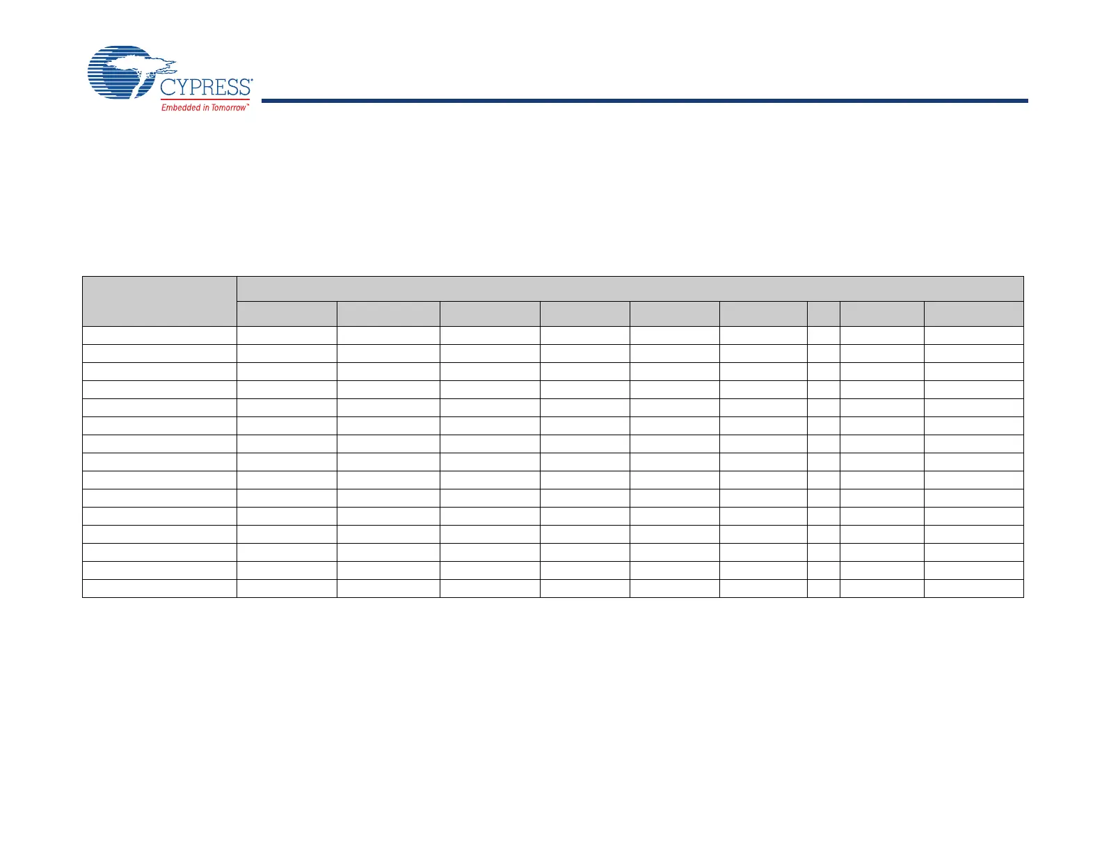
Table 19. GPIO Multiplexing Matrix
Pin Name
Pad Function Control Register Setting
0 1 2 3 4 5 6 7 15
BT_UART_CTS_N UART_CTS_N – – – – – – A_GPIO[1] –
BT_UART_RTS_N UART_RTS_N – – – – – – A_GPIO[0] –
BT_UART_RXD UART_RXD – – – – – – GPIO[5] –
BT_UART_TXD UART_TXD – – – – – – GPIO[4] –
BT_PCM_IN A_GPIO[3] PCM_IN PCM_IN HCLK – – – I2S_SSDI/MSDI SF_MISO
BT_PCM_OUT A_GPIO[2] PCM_OUT PCM_OUT LINK_IND – I2S_MSDO – I2S_SSDO SF_MOSI
BT_PCM_SYNC A_GPIO[1] PCM_SYNC PCM_SYNC HCLK INT_LPO I2S_MWS – I2S_SWS SF_SPI_CSN
BT_PCM_CLK A_GPIO[0] PCM_CLK PCM_CLK – – I2S_MSCK – I2S_SSCK SF_SPI_CLK
BT_I2S_DO A_GPIO[5] PCM_OUT – – I2S_SSDO I2S_MSDO – STATUS –
BT_I2S_DI A_GPIO[6] PCM_IN – HCLK I2S_SSDI/MSDI – – TX_CON_FX –
BT_I2S_WS GPIO[7] PCM_SYNC – LINK_IND – I2S_MWS – I2S_SWS –
BT_I2S_CLK GPIO[6] PCM_CLK – – INT_LPO I2S_MSCK – I2S_SSCK –
BT_GPIO_1 GPIO[1] – – – – – – CLASS1[2] –
BT_GPIO_0 GPIO[0] – – – clk_12p288 – – – –
CLK_REQ WL/BT_CLK_REQ – – – – – – A_GPIO[7] –


 To Next Page