107
TOP258MG (SMPS : IC601)
Pin Functional Description
DRAIN (D) Pin:
High-voltage power MOSFET DRAIN pin. The internal start-up
bias current is drawn from this pin through a switched high-
voltage current source. Internal current limit sense point for
drain current.
CONTROL (C) Pin:
Error amplifi er and feedback current input pin for duty cycle
control. Internal shunt regulator connection to provide internal
bias current during normal operation. It is also used as the
connection point for the supply bypass and auto-restart/
compensation capacitor.
EXTERNAL CURRENT
LIMIT (X) Pin (Y, M, E and L package):
Input pin for external current limit adjustment and remote
ON/OFF. A connection to SOURCE pin disables all functions
on this pin.
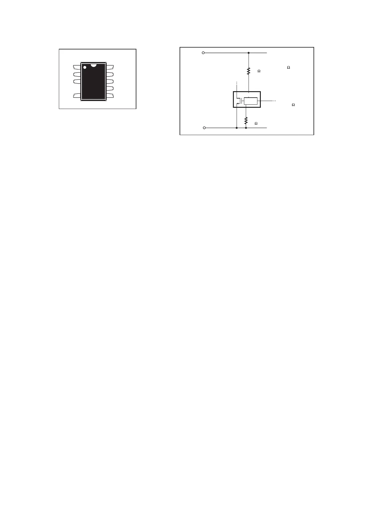
X
PI-4711-021308
DC
Input
Voltage
+
-
D
S
C
CONTROL
V
R
IL
R
LS
12 k
4 M
V
UV
= I
UV
× R
LS
+ V
V
(I
V
= I
UV
)
V
OV
= I
OV
× R
LS
+ V
V
(I
V
= I
OV
)
For R
LS
= 4 M
DC
MAX
@100 VDC = 76%
DC
MAX
@375 VDC = 41%
For R
IL
= 12 k
I
LIMIT
= 61%
See Figure 55b for
other resistor values
(R
IL
) to select different
I
LIMIT
values.
V
UV
= 102.8 VDC
V
OV
= 451 VDC
Figure 5. TOP254-258 Y and All M/E/L Package Line Sense and Externally Set
Current Limit.
VOLTAGE MONITOR (V) Pin (Y & M package only):
Input for OV, UV, line feed forward with DC
MAX
reduction, output
overvoltage protection (OVP), remote ON/OFF and device reset.
A connection to the SOURCE pin disables all functions on this pin.
MULTI-FUNCTION (M) Pin (P & G packages only):
This pin combines the functions of the VOLTAGE MONITOR (V)
and EXTERNAL CURRENT LIMIT (X) pins of the Y package into
one pin. Input pin for OV, UV, line feed forward with DC
MAX
S
S
S
S
S
M Package
D
X
C
V
10
6
9
1
5
8
7
2
3
reduction, output overvoltage protection (OVP), external current
limit adjustment, remote ON/OFF and device reset. A
connection to SOURCE pin disables all functions on this pin
and makes TOPSwitch-HX operate in simple three terminal
mode (like TOPSwitch-II).
FREQUENCY (F) Pin (TOP254-258Y, and all E and L packages):
Input pin for selecting switching frequency 132 kHz if connected
to SOURCE pin and 66 kHz if connected to CONTROL pin.
The switching frequency is internally set for fi xed 66 kHz
operatio
n in the P, G, M package and TOP259YN, TOP260YN
and TOP261YN.
SIGNAL GROUND (G) Pin (TOP259YN, TOP260YN &
TOP261YN only):
Return for C pin capacitor and X pin resistor.
SOURCE (S) Pin:
Output MOSFET source connection for high voltage power
return. Primary side control circuit common and reference point.
 Loading...