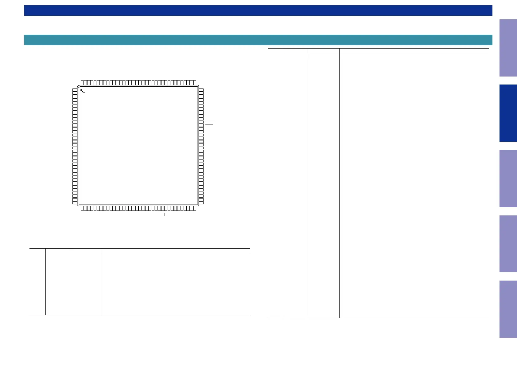
1. IC's
ADV7623 (DIGITAL_HDMI_ADV7623 : IC731)
ADV7623
TOP VIEW
(Not to Scale)
PIN 1
1
DDCC_SCL
2
3
4
5
6
7
8
9
10
11
12
13
14
15
16
17
18
19
20
21
22
23
24
25
26
27
28
29
30
31
32
33
34
35
36
73
DVDDIO
74
AP3_IN
75
AP2_IN
76
AP1_IN
77
AP0_IN
78
SDATA
79
SCL
80
DGND
81
DVDD
82
INT1
83
INT2
84
INT_TX
85
DGNDIO
86
DVDDIO
87
AP0_OUT
88
AP1_OUT
89
AP2_OUT
90
AP3_OUT
91
AP4_OUT
92
DGND
93
DVDD
94
AP5_OUT
95
SCLK_OUT
96
MCLK_OUT
97
RESET
98
PWRDN
99
PGND
100
PVDD
101
XTAL
102
XTAL1
103
PVDD
104
PGND
105
HP_CTRLA
106
5V_DETA
107
RTERM
108
DDCA_SDA
109
110
111
112
113
114
115
116
117
118
119
120
121
122
123
124
125
126
127
128
129
130
131
132
133
134
135
136
137
138
139
140
141
142
143
144
DDCC_SDA
37
TXPLVDD
38
TXGND
39
TXPGND
40
41
42
43
44
45
46
47
48
49
50
51
52
53
54
55
56
57
58
59
60
61
62
63
64
65
66
67
68
69
70
71
72
EXT_SWING
HPD_ARC–
ARC+
XDDC_SD
TXDDC_SCL
TXAVDD
TXGND
TXC–
TXC+
TXGND
TX0–
TX0+
TXGND
TX1–
TX1+
TXAVDD
TX2–
TX2+
TXGND
CEC
DGND
DVDD
ALSB
CS
EP_SCK
EP_CS
EP_MOSI
EP_MISO
MCLK_IN
SCLK_IN
AP5_IN
AP4_IN
DGNDIO
5V_DETC
HP_CTRLC
RXB_2+
RXB_2–
TVDD
RXB_1+
RXB_1–
CGND
RXB_0+
RXB_0–
TVDD
RXB_C+
RXB_C–
CGND
CVDD
DDCB_SCL
DDCB_SDA
DVDD
DGND
5V_DETB
HP_CTRLB
RXA_2+
RXA_2–
TVDD
RXA_1+
RXA_1–
CGND
RXA_0+
RXA_0–
TVDD
RXA_C+
RXA_C–
CGND
CVDD
DDCA_SCL
CVDD
CGND
RXC_C–
RXC_C+
TVDD
RXC_0–
RXC_0+
CGND
RXC_1–
RXC_1+
TVDD
RXC_2–
RXC_2+
HP_CTRLD
5V_DETD
DGND
DVDD
DDCD_SD
DDCD_SCL
CVDD
CGND
RXD_C–
RXD_C+
TVDD
RXD_0–
RXD_0+
CGND
RXD_1–
RXD_1+
TVDD
RXD_2–
RXD_2+
CVDD
CGND
TXPVDD
Pin Function Descriptions
Pin No. Mnemonic Type Description
1 DDCC_SCL Digital input HDCP Slave Serial Clock Port C. DDCC_SCL is a 3.3 V input that is 5 V tolerant.
2 CVDD Power Receiver Comparator Supply Voltage (1.8 V).
3 CGND Ground TVDD and CVDD Ground.
4 RXC_C− HDMI input Digital Input Clock Complement of Port C in the HDMI Interface.
5 RXC_C+ HDMI input Digital Input Clock True of Port C in the HDMI Interface.
6 TVDD Power Receiver Terminator Supply Voltage (3.3 V).
7 RXC_0− HDMI input Digital Input Channel 0 Complement of Port C in the HDMI Interface.
8 RXC_0+ HDMI input Digital Input Channel 0 True of Port C in the HDMI Interface.
9 CGND Ground TVDD and CVDD Ground.
10 RXC_1− HDMI input Digital Input Channel 1 Complement of Port C in the HDMI Interface.
11 RXC_1+ HDMI input Digital Input Channel 1 True of Port C in the HDMI Interface.
12 TVDD Power Receiver Terminator Supply Voltage (3.3 V).
Pin No. Mnemonic Type Description
13 RXC_2− HDMI input Digital Input Channel 2 Complement of Port C in the HDMI Interface.
14 RXC_2+ HDMI input Digital Input Channel 2 True of Port C in the HDMI Interface.
15 HP_CTRLD Digital output Hot Plug Detect for Port D.
16 5V_DETD Digital input 5 V Detect Pin for Port D in the HDMI Interface.
17 DGND Ground DVDD Ground.
18 DVDD Power Digital Supply Voltage (1.8 V).
19 DDCD_SDA Digital I/O HDCP Slave Serial Data Port D. DDCD_SDA is a 3.3 V input/output that is 5 V tolerant.
20 DDCD_SCL Digital input HDCP Slave Serial Clock Port D. DDCD_SCL is a 3.3 V input that is 5 V tolerant.
21 CVDD Power Receiver Comparator Supply Voltage (1.8 V).
22 CGND Ground TVDD and CVDD Ground.
23 RXD_C− HDMI input Digital Input Clock Complement of Port D in the HDMI Interface.
24 RXD_C+ HDMI input Digital Input Clock True of Port D in the HDMI Interface.
25 TVDD Power Receiver Terminator Supply Voltage (3.3 V).
26 RXD_0− HDMI input Digital Input Channel 0 Complement of Port D in the HDMI Interface.
27 RXD_0+ HDMI input Digital Input Channel 0 True of Port D in the HDMI Interface.
28 CGND Ground TVDD and CVDD Ground.
29 RXD_1− HDMI input Digital Input Channel 1 Complement of Port D in the HDMI Interface.
30 RXD_1+ HDMI input Digital Input Channel 1 True of Port D in the HDMI Interface.
31 TVDD Power Receiver Terminator Supply Voltage (3.3 V).
32 RXD_2− HDMI input Digital Input Channel 2 Complement of Port D in the HDMI Interface.
33 RXD_2+ HDMI input Digital Input Channel 2 True of Port D in the HDMI Interface.
34 CVDD Power Receiver Comparator Supply Voltage (1.8 V).
35 CGND Ground TVDD and CVDD Ground.
36 TXPVDD Power
1.8 V Power Supply for Digital and I/O Power Supply. This pin supplies power to the
digital logic and I/Os. It should be ltered and as quiet as possible.
37 TXPLVDD Power 1.8 V Power Supply.
38 TXGND Ground TXPVDD Ground.
39 TXPGND Ground TXPLVDD Ground.
40 EXT_SWING Analog input
This pin sets the internal reference currents. Place an 887 Ω resistor (1% tolerance) between
this pin and ground.
41 HPD_ARC− Analog input
Hot Plug Detect Signal. This pin indicates to the interface whether the receiver is connected.
It supports 1.8 V to 5 V CMOS logic levels.
42 ARC+ Analog input Audio Return Channel Input (5 V Tolerant).
43 TXDDC_SDA Digital I/O
Serial Port Data I/O to Receiver. This pin serves as the master to the DDC bus. It supports a
5 V CMOS logic level.
44 TXDDC_SCL Digital output
Serial Port Data Clock to Receiver. This pin serves as the master clock for the DDC bus.
It supports a 5 V CMOS logic level.
45 TXAVDD Power 1.8 V Power Supply for TMDS Outputs.
46 TXGND Ground TXAVDD Ground.
47 TXC− HDMI output
Dierential Clock Output. Dierential clock output at the TMDS clock rate; supports
TMDS logic level.
48 TXC+ HDMI output
Dierential Clock Output. Dierential clock output at the TMDS clock rate; supports
TMDS logic level.
49 TXGND Ground TXAVDD Ground.
50 TX0− HDMI output
Dierential Output Channel 0 Complement. Dierential output of the red data at 10×
the pixel clock rate; supports TMDS logic level.
51 TX0+ HDMI output
Dierential Output Channel 0 True. Dierential output of the red data at 10× the pixel clock
rate; supports TMDS logic level.
52 TXGND Ground TXAVDD Ground.
53 TX1− HDMI output
Dierential Output Channel 1 Complement. Dierential output of the red data at 10×
the pixel clock rate; supports TMDS logic level.
54 TX1+ HDMI output
Dierential Output Channel 1 True. Dierential output of the red data at 10× the pixel
clock rate; supports TMDS logic level.
55 TXAVDD Power 1.8 V Power Supply for TMDS Outputs.
SEMICONDUCTORS
Only major semiconductors are shown, general semiconductors etc. are omitted to list.
The semiconductor which described a detailed drawing in a schematic diagram are omitted to list.
39
Caution in
servicing
Electrical Mechanical Repair Information Updating
 Loading...