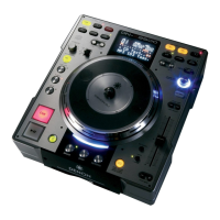
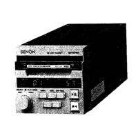
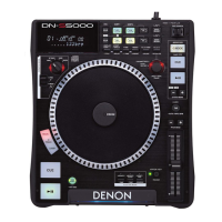
20
20DN-S5000
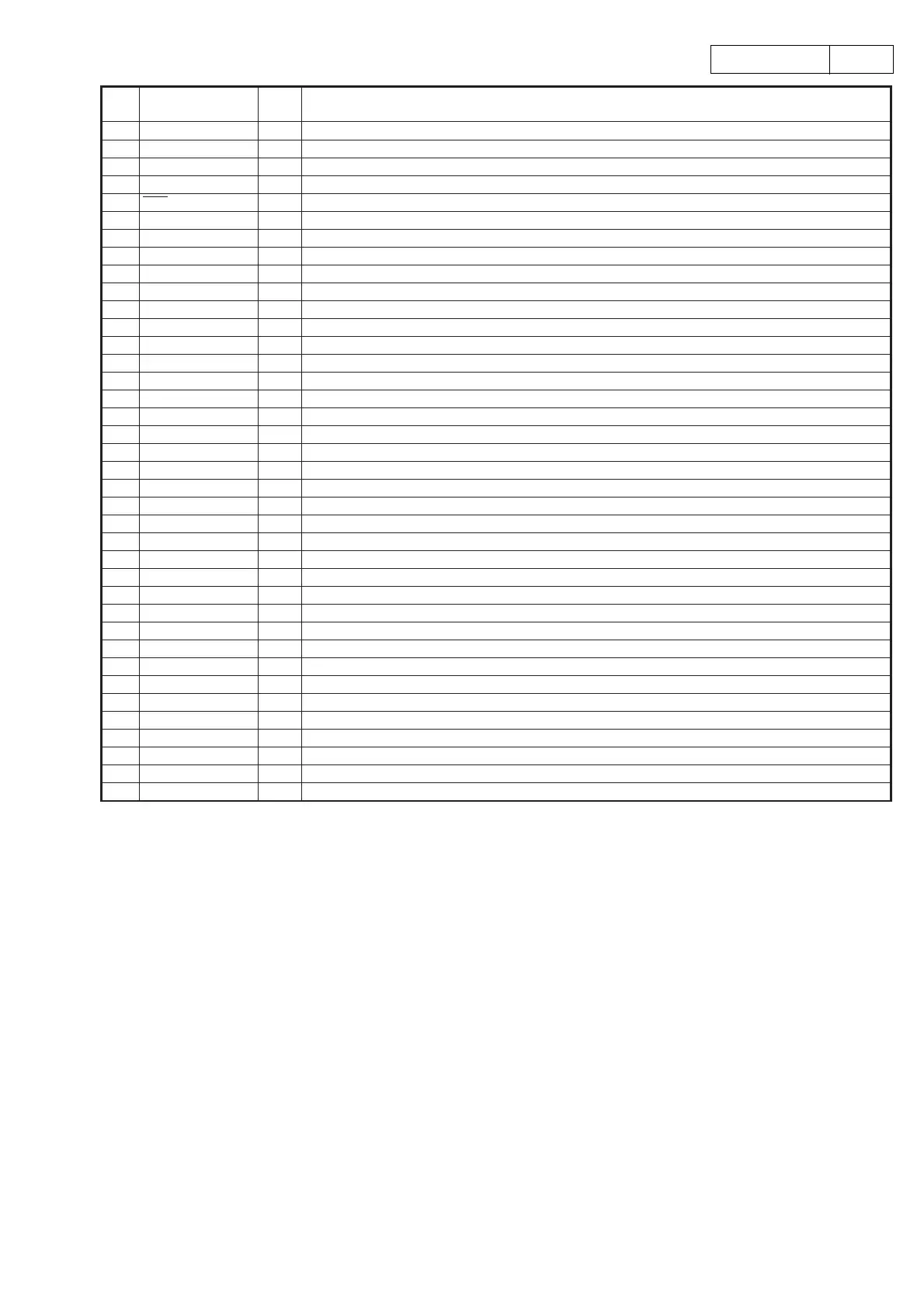
Note: (1) Schmitt-Trigger input with internal pull-down, 5V tolerant. (2) Schmitt-Trigger input, 5V tolerant. (3) Tri-state output.
Function
Pin
No.
Pin Name
I/O
11 V
OUT
4 O Voltage Output of Audio Signal Corresponding to Rch on DATA2. Up to 96kHz
12 V
OUT
3 O Voltage Output of Audio Signal Corresponding to Rch on DATA2. Up to 96kHz
13 V
OUT
2 O Voltage Output of Audio Signal Corresponding to Rch on DATA1. Up to 192kHz
14 V
OUT
1 O Voltage Output of Audio Signal Corresponding to Rch on DATA1. Up to 192kHz
15 V
COM
O Common Voltage Output. This pin should be bypassed with a 10µF capacitor to AGND
16 V
OUT
7 O Voltage Output for Audio Signal Corresponding to Rch on DATA4. Up to 192kHz
17 AGND5 — Analog Ground
18 V
CC
5 — Analog Power Supply, +5V
19 AGND6 — Analog Ground
20 V
OUT
8 — Voltage Output for Audio Signal Corresponding to Rch on DATA4. Up to 192kHz
21 AGND4 — Analog Ground
22 V
CC
4 — Analog Power Supply, +5V
23 AGND3 — Analog Ground
24 V
CC
3 — Analog Power Supply, +5V
25 AGND2 — Analog Ground
26 V
CC
2 — Analog Power Supply, +5V
27 AGND1 — Analog Ground
28 V
CC
1 — Analog Power Supply, +5V
29 NC — No Connection
30 ZERO7 — Zero Data Flag for V
OUT
7
31 DATA4 — Serial Audio Data Input V
OUT
7 and V
OUT
8
(2)
32 ZERO8 — Zero Data Flag for V
OUT
7
33 MDO O Serial Audio Data Output for Serial Port
(3)
34 MDI l Serial Audio Data Input for Serial Port
(1)
35 MC l Shift Clock for Serial Control Port
(1)
36
ML l Latch Enable for Serial Control Port
(1)
37 RST l System Reset, Active LOW
(1)
38 SCKI l System Clock Input frequency is 128,192,256,384,512,or 768fs.
(2)
39 SCKO O Buffered Clock Output frequency is 128,192,256,384,512,or 768fs.
(2)
40 BCK l Shift Clock Input for Serial Audio Data. Clock must be 32,48,or,64fs.
(2)
41 LRCK l Left and Right Clock Input. This clock is equal to the sampling rate, fs.
(2)
42 TEST — Test Pin. This pin should be connected to DGND.
(1)
43 V
DD
— Digital Power Supply, +3.3V
44 DGND — Digital Ground
45 DATA1 l Serial Audio Data Input V
OUT
1 and V
OUT
2
(2)
46 DATA2 l Serial Audio Data Input V
OUT
3 and V
OUT
4
(2)
47 DATA3 l Serial Audio Data Input V
OUT
5 and V
OUT
6
(2)
48 ZEROA O Zero Data Flag. Logical “AND” of ZERO1 through ZERO6
 Loading...