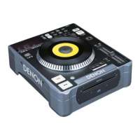
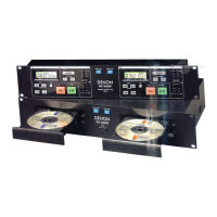
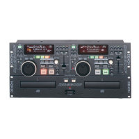
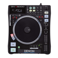
10
10DN-S5000
SEMICONDUCTORS
z IC's
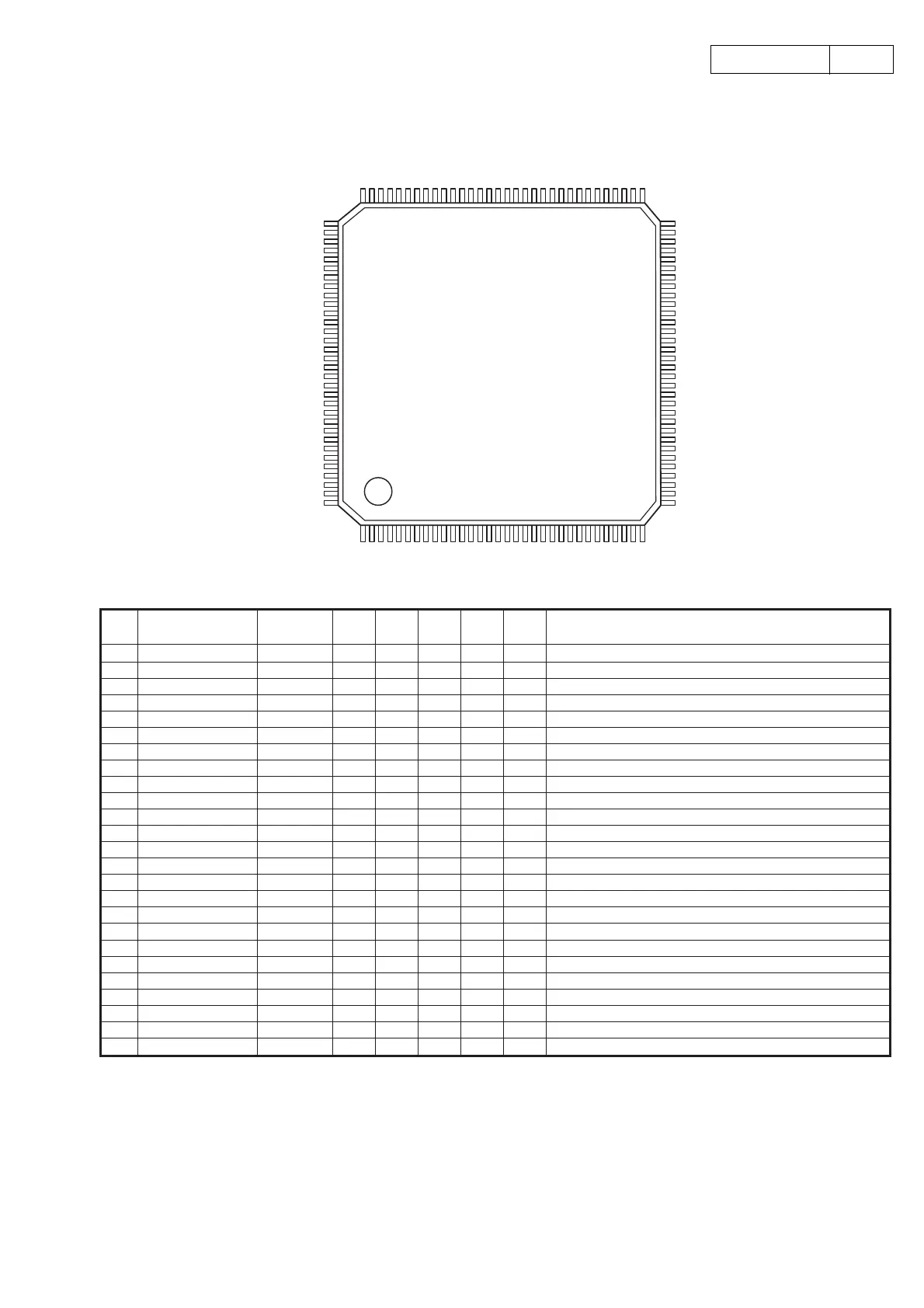
MN102H730F (IC501)
MN102H730F Terminal Function
128 33
97 64
132
96 65
TOP VIEW
Function
I/O
Pin
No.
Pin Name
Symbol
1 CS0_ CS0_ O — Pu — — Ext. memory chip select 0 (Flash ROM CS)
2 CS1_ CS1_ O — Pu — — Ext. memory chip select 1 (Flash ROM for memo)
3 D00 DQ0 I/O — — — — Ext. memory data in/output 0, DSP interface 0
4 D01 DQ1 I/O — — — — Ext. memory data in/output 1, DSP interface 1
5 D02 DQ2 I/O — — — — Ext. memory data in/output 2, DSP interface 2
6 D03 DQ3 I/O — — — — Ext. memory data in/output 3, DSP interface 3
7 VDD VDD — — — — —
Power (+3.3V)
8 VSS VSS — — — — — GND
9 D04 DQ4 I/O — — — — Ext. memory data in/output 4, DSP interface 4
10 D05 DQ5 I/O — — — — Ext. memory data in/output 5, DSP interface 5
11 D06 DQ6 I/O — — — — Ext. memory data in/output 6, DSP interface 6
12 D07 DQ7 I/O
I/O
— — — — Ext. memory data in/output 7, DSP interface 7
13 D08 DQ8 — — —
14 D09 DQ9 — — —
15 D10 DQ10 — — —
16 PD0,DMAACK1_ RESERVE —
17 PD1,DMAREQ1_ RESERVE —
L—
L—
18 D11 DQ11 — — —
19 D12 DQ12 — — —
20 D13 DQ13 — — —
21 D14 DQ14 — — —
22 D15 DQ15 — — —
23 WORD WORD I — — Data bus width select (H: 16bit), GND fixed
24 VDD VDD — — — — — Power (+3.3V)
25 MODE MODE I — — L L Processor mode, GND fixed
DET Ext Ini Res
—
I/O
I/O
O
O
I/O
I/O
I/O
I/O
I/O
—
—
—
—
—
—
—
—
—
Ext. memory data in/output 8, DSP interface 8
Ext. memory data in/output 9, DSP interface 9
Ext. memory data in/output 10, DSP interface 10
Ext. memory data in/output 11, DSP interface 11
Ext. memory data in/output 12, DSP interface 12
Ext. memory data in/output 13, DSP interface 13
Ext. memory data in/output 14, DSP interface 14
Ext. memory data in/output 15, DSP interface 15
 Loading...