EasyManua.ls Logo

Denon DN-X1500 Service Manual

Denon DN-X1500
60 pages
To Next Page IconTo Next Page
Page #1 background imageLoading...
Page #1 background image
SERVICE MANUAL
MODEL
DN-X1500
DJ MIXER
For U.S.A., Canada, Europe,
Oceania & Asia model
16-11, YUSHIMA 3-CHOME, BUNKYO-KU, TOKYO 113-0034 JAPAN
X-0196V.01 DE/CDM 0401
注 意
サービスをおこなう前に、このサービスマニュアルを
必ずお読みください。本機は、火災、感電、けがなど
に対する安全性を確保するために、さまざまな配慮を
おこなっており、また法的には「電気用品安全法」に
もとづき、所定の許可を得て製造されております。
従ってサービスをおこなう際は、これらの安全性が維
持されるよう、このサービスマニュアルに記載されて
いる注意事項を必ずお守りください。
本機の仕様は性能改良のため、予告なく変更すること
があります。
補修用性能部品の保有期間は、製造打切後
8年です。
Some illustrations using in this service manual are
slightly different from the actual set.
Please use this service manual with referring to
the operating instructions without fail.
For purposes of improvement, specifications and
design are subject to change without notice.
修理の際は、必ず取扱説明書を参照の上、作業を行って,
ください。
本文中に使用しているイラストは、説明の都合上現物
と多少異なる場合があります。
Ver. 1

Other manuals for Denon DN-X1500

Question and Answer IconNeed help?

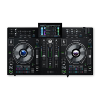
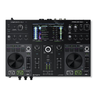
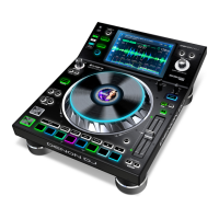
Do you have a question about the Denon DN-X1500 and is the answer not in the manual?

Denon DN-X1500 Specifications

General IconGeneral
BrandDenon
ModelDN-X1500
CategoryDJ Equipment
LanguageEnglish

Summary

Service Manual Overview

Safety Precautions

Leakage Current and Laser Safety Checks

Details essential safety checks, including leakage current and laser radiation, for technician and user protection.

Disassembly Procedures

Top Panel and Cross Feder Unit Removal

Step-by-step guide for disassembling the top panel and cross fader unit.

CH Fader and Front Panel Disassembly

Instructions for removing the CH fader unit and front panel components.

Service Mode Specifications

Power On and Level Meter Operations

Details on entering service mode, power control, and CH/Master level meter functions.

Crossfader and µ Com Version Checks

Explains crossfader assign modes and how to perform µ Com version checks.

Semiconductor Component Details

MN102H74D Microcontroller Pinout

Detailed pin functions for the MN102H74D microcontroller (IC101).

Audio Codec and Interface ICs

Descriptions for AD1838A Audio Codec, AK4103A Audio Interface, and related ICs.

Display Driver IC Functions

Details terminal functions and block diagram for the M66005AFP display driver (IC201).

FL Display and Connection Details

FL Display Pin Connections

Shows pin connection details for the FL DISPLAY 16-ST-73GN (FL201).

FL Display Grid Assignments

Illustrates the grid assignments for the FL DISPLAY 16-ST-73GN (FL201).

Anode Connection Details

Printed Wiring Board Layouts

GU-3591 Main/Power PWB Component Side

Component layout diagram for the GU-3591 Main/Power PWB.

GU-3591 Main/Power PWB Foil Side

Foil side layout diagram for the GU-3591 Main/Power PWB.

GU-3592 P.uCOM/Input PWB Layouts

Component and foil side layout diagrams for the GU-3592 P.uCOM/Input PWB.

GU-3593 P.VR PWB Layouts

Component and foil side layout diagrams for the GU-3593 P.VR PWB.

GU-3594 DSP PWB Layouts

Component and foil side layout diagrams for the GU-3594 DSP PWB.

Parts List Information

Parts List - Main/Power PWB

Semiconductor Components (GU-3591)

List of semiconductor components used in the GU-3591 Main/Power PWB unit.

Resistors and Transistors (GU-3591)

List of resistors and transistors for the GU-3591 Main/Power PWB unit.

Parts List - Capacitors and Resistors

Capacitors Group (GU-3591)

List of capacitors used in the GU-3591 Main/Power PWB unit.

Resistors Group (GU-3591)

List of resistors used in the GU-3591 Main/Power PWB unit.

Exploded View and Parts List

Exploded View Diagram

Visual representation of the product's assembly with numbered parts.

Parts List for Exploded View

List of parts corresponding to the exploded view diagram.

Packing and Accessories List

Block Diagram - Audio Part

Block Diagram - System Part

Level Diagram

Wiring Diagram

Notes for Schematic Diagrams

Schematic Diagrams (1/8)

GU-3591 Main Unit - Microcontroller Block

Schematic for the GU-3591 Main Unit, focusing on the main microcontroller (uCOM) block.

Schematic Diagrams (2/8)

GU-3591 Main Unit - Audio A/D D/A Block

Schematic for the GU-3591 Main Unit, detailing the Audio A/D and D/A conversion blocks.

Schematic Diagrams (3/8)

GU-3591 Main Unit - Output Block

Schematic for the GU-3591 Main Unit, illustrating the output stages and related circuitry.

Schematic Diagrams (4/8)

GU-3591 Power and Trans Units

Schematics for the GU-3591 Power Unit and Trans Unit, including power supply and voltage regulation.

Schematic Diagrams (5/8)

GU-3592 P.uCOM and Related Units

Schematics for GU-3592 P.uCOM Unit and related input/switch units.

Schematic Diagrams (6/8)

GU-3592 Input Unit Details

Schematic focused on the GU-3592 Input Unit, showing input circuitry and selectors.

Schematic Diagrams (7/8)

GU-3593 P.VR and Fader Units

Schematics for the GU-3593 P.VR Unit and its associated CH Fader Units.

Schematic Diagrams (8/8)

GU-3594 DSP Unit Details

Schematic for the GU-3594 DSP Unit, detailing the DSP and memory interface.

Related product manuals