18
18UD-M31
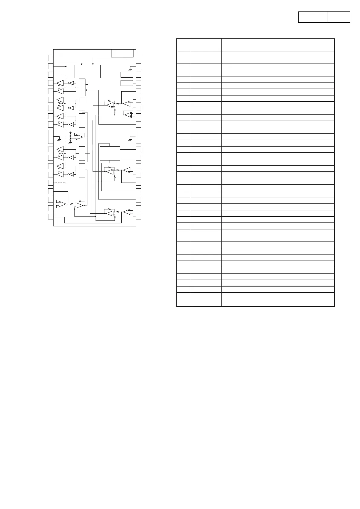
LA6559(IC801)
1 REV
5CH output change terminal, logic input of
loading block
2 S-Vcc
signal system power supply
(BTL-AMP:CH1~4)
3 Vcc2 Power supply for loading block
4 VLO- Loading output (-)
5 VL0+ Loading output (+)
6 VO4+ Output terminal (+) for channel 4
7 VO4- Output terminal ( ) for channel 4
8 VO3+ Output terminal (+) for channel 3
9 VO3- Output terminal (- ) for channel 3
10 VO2+ Output terminal (+) for channel 2
11 VO2- Output terminal (- ) for channel 2
12 VO1+ Output terminal (+) for channel 1
13 VO1- Output terminal (- ) for channel 1
14 Vcc1 CH1 `CH4(BTL-AMP) output stage power supply
15 VIN1 Input terminal for channel 1
16 VIN1- OP-AMP input AMP-A input terminal (- )
17 VIN1+ OP-AMP input AMP-A input terminal (+)
18 VIN2 Input terminal for channel 2, input AMP output
19 VIN2- Input terminal (- ) for channel 2
20 VIN2+ Input terminal (+) for channel 2
21 Vcc-VREG 3.3VREG power supply
22 GND-VREG 3.3VREG GND
23 VIN3 Input terminal for channel 3, input AMP output
24 VIN3- Input terminal (- ) for channel 3
25 VIN3+ Input terminal (+) for channel 3
26 REG-IN PNP transistor base connected
27 REG-OUT
3.3V power output to which the PNP transistor
collector connected
28 VCONT Loading output voltage set terminal
29 VREF-IN Reference voltage applied terminal
30 VIN4+ Input terminal (+) for channel 4
31 VIN4- Input terminal (- ) for channel 4
32 VIN4 Input terminal for channel 4, input AMP output
33 MUTE1 Output ON/OFF for channel 1 (BTL AMP)
34 MUTE2 Output ON/OFF for channel 2 to 4 (BTL AMP)
35 S-GND Signal system GND
36 FWD
Output change terminal (FWD) for loading
output (VLO+,-), logic input of loading block
Pin
No.
Name
Function
1
2
3
4
5
6
7
8
9
FR
10
11
12
13
14
15
16
17
18
36
35
34
33
32
31
30
29
28
FR
27
26
25
24
23
22
21
20
19
FWD
S-GND
MUTE2
MUTE1
VIN4
VIN4-
VIN4+
VREF-IN
VCONT(LOADING)
FR
REG-OUT
REG-IN
VIN3+
VIN3-
VIN3
GND-VREG
VCC-VREG
VIN2+
VIN2-
REV
S-VCC
VCC2
VLO-
VLO+
VO4+
VO4-
VO3+
VO3-
FR
VO2+
VO2-
VO1+
VO1-
VCC1
VIN1
VIN1-
VIN1+
VIN2
Signal System VCC
(CH1 to CH4)
33k
11k
33k
11k
3.3VREG GND
3.3VREG
33k
11k
3.3VREG
PNP Tr
Base
PNP Tr
Collector
33k
11k
CH1 Output
ON/OFF
CH2 to CH4
Output
MUTE1
MUTE2
(LOADING)
Power Supply
Input
(Forward/Reverse/
Break/OFF)
Output
Control
Level
Shift
Level
Shift
Power
System
GND
Level
Shift
Level
Shift
Power Supply
Power Supply
(External PNP)
Power System GND
Signal System GND
Thermal
Shutdown
-
)
S
11k
PNP Tr
Base
11k
t
(LOADING)
Power Supply
Input
(For rd/Reverse/
Output
Power
System
ft
u
)
T
Sh
 Loading...