Design notes Design notes for RF pad devices
Digi XBee® 3 RF Module Hardware Reference Manual
37
Number Description
1
Maintain a distance of at least 2 d between microstrip and ground fill.
2 RF pad pin.
3 50 Ω microstrip trace.
4 RF connection of RPSMA jack.
This example is on a surface-mount device. The width in this example is approximately 0.045" for a 50
Ω trace, assuming d=0.025”, and that the dielectric has a relative permittivity of 4.4. This trace width
is a good fit with the device footprint's 0.060" pad width.
Note We do not recommend using a trace wider than the pad width, and using a very narrow trace
(under 0.010") can cause unwanted RF loss.
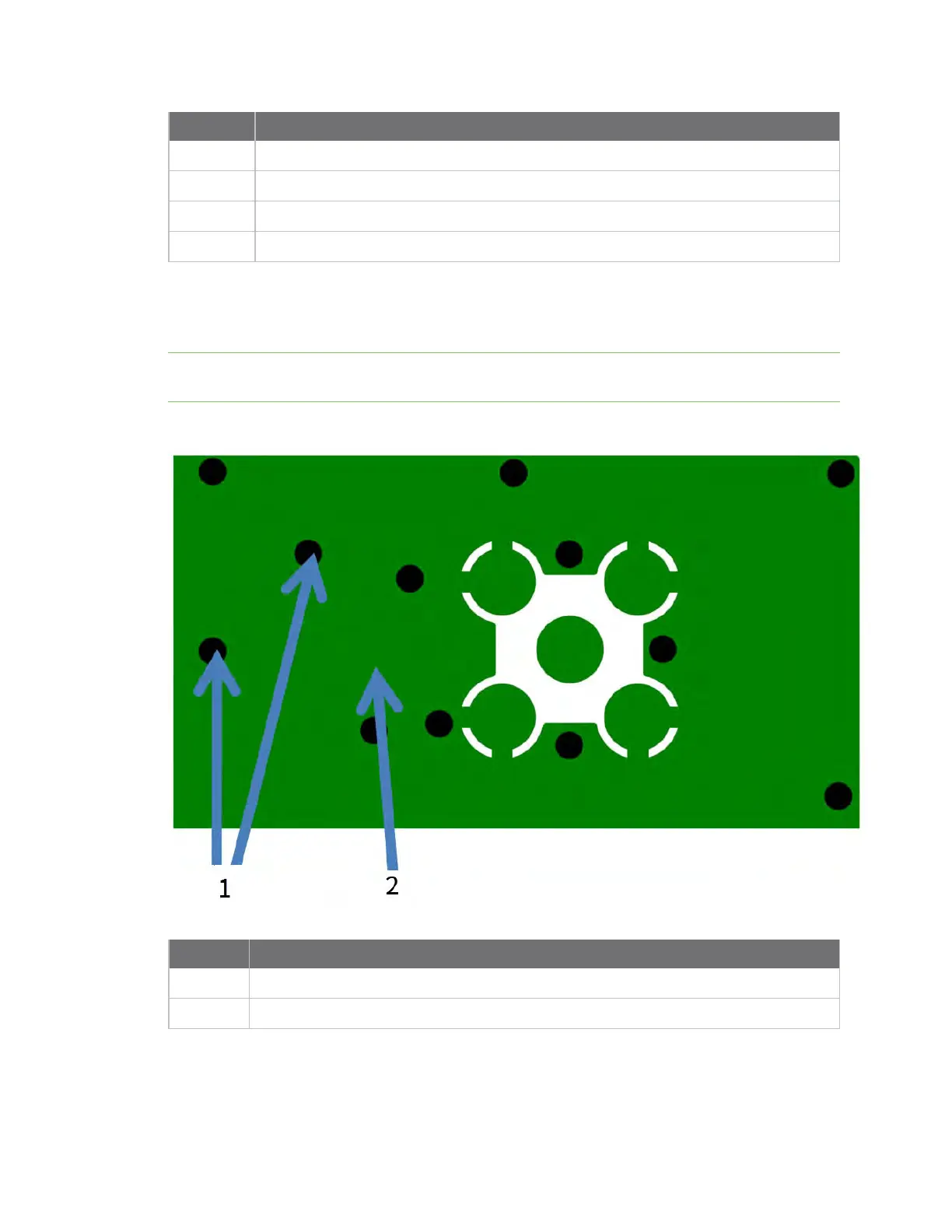
The following illustration shows PCB layer 2 of an example RF layout.
Number Description
1
Use multiple vias to help eliminate ground variations.
2 Put a solid ground plane under RF trace to achieve the desired impedance.
 Loading...