Advanced Function Instruction
7-11
FUN32
ADCNV
CONVERTING THE RAW VALUE OF 4~20MA ANALOG INPUT
(ADCNV)
FUN32
ADCNV
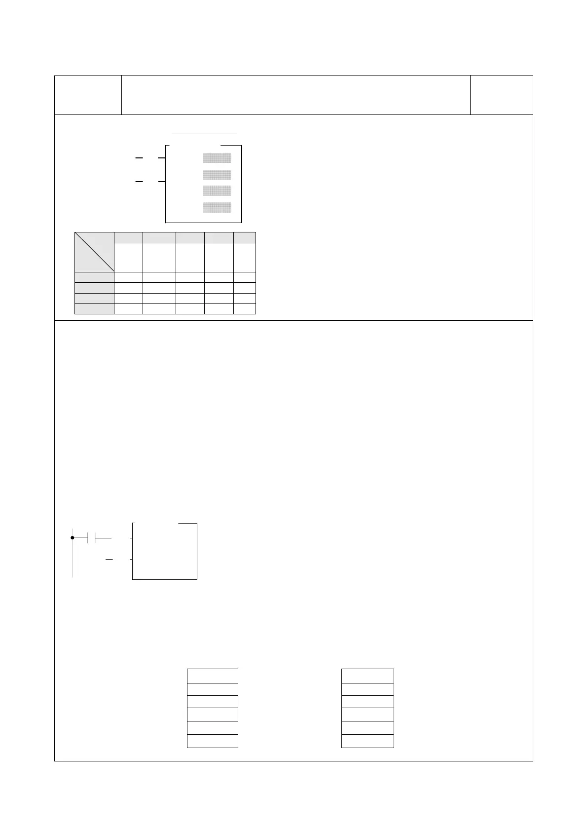
Pl :
N :
EN
Ladder symbol
32.ADCNV
S :
D :
F/T
Operation Control
14/12 - Bit Selection
HR IR ROR DR K
Range
Ope-
rand
R0
∣
R3839
R3840
∣
R3903
R5000
∣
R8071
D0
∣
D4095
Pl 0~1
S ○ ○ ○ ○
N ○ ○ ○ 1~64
D ○ ○* ○
Pl:0, the polarity setting of analog input module is at unipolar
position
:1, the polarity setting of analog input module is at bipolar
position
S:Starting address of source registers
N:Quantity of conversion (In Word)
D:Starting address of destination registers
S, N, D may associate with V、Z、P0~P9 index register to serve
the indirect addressing application.
● When the analog input is 4~20mA, the analog input module is one of the solution to get this kind of signal,
but the input span of the analog input module is 0~20mA (Setting at 10V、Unipolar), however there will exist
the offset of the raw reading value; this instruction is applied to eliminate the offset and convert the raw
reading value into the range of 0~4095(12-bit) or 0~16383(14-bit), it is more convenient for following
operation.
● When execution control "EN"=1, it will execute the conversion starting from S, length by N, and then store
the results into the D registers.
● This instruction will not act if invalid length of N.
● When the input〝F/T〞=0, it assigns the 12-bit analog input module; while〝F/T〞=1, it assigns the 14-bit
analog input module.
Example:
M0
32.ADSNV
EN
N :
D :
S :
F/T
P1 :
0
R3840
R500
6
Description:When M0 is ON, it will perfom 6 points of conversion starting from R3840, where the offset of 4~
20mA raw reading value will be eliminated, and the corresponding value 0~4095 will be stored into
R500~R505.
S D
R3840
-1229
R500
0
(4 mA)
R3841 409 R501 2047 (12 mA)
R3842 2047 R502 4095 (20 mA)
R3843
-2048
R503 0 (0 mA)
R3844
-2048
R504 0 (0 mA)
R3845
-2048
Ö
R505 0 (0 mA)