Chapter 3 -- Instrument Circuitry--eQCM 10M Schematic/Block Diagram
3 - 3
Chapter 3 -- Instrument Circuitry
eQCM 10M Schematic/Block Diagram
If you are not familiar with electronic schematics or quartz crystal microbalances, you probably want to skip this
chapter. This information is for expert use only and is not required for routine use of the instrument.
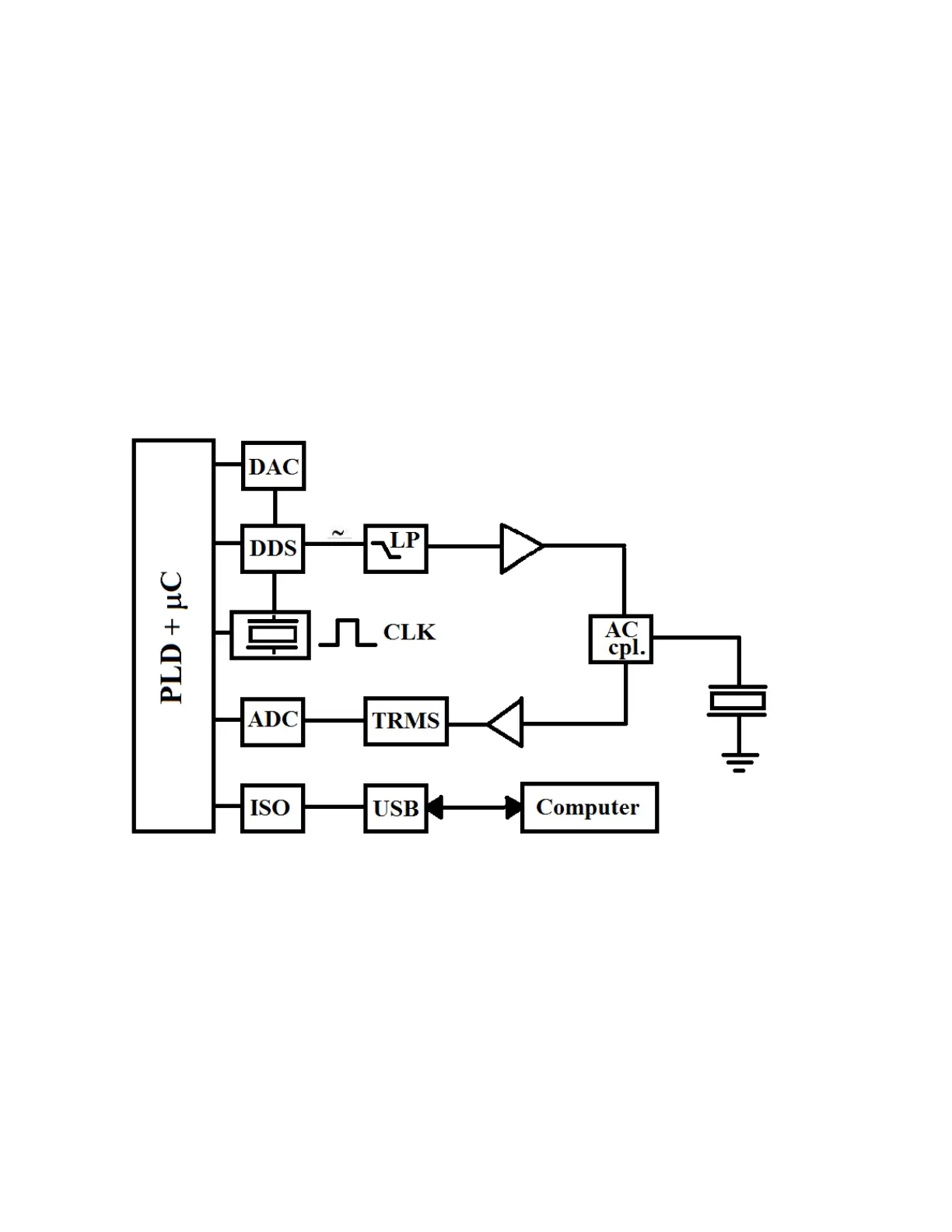
The following figure is part schematic diagram and part block diagram. They are intended to show the basic
principles of the instrument without the confusion of the full circuitry details.
The schematic/block diagram figure shows the quartz crystal microbalance board.
Figure 3-1
eQCM 10M Impedance Scanning Quartz Crystal Microbalance Board
Simplified Schematic/Block Diagram
Notes for Figure 3-1
• The programmable logic device (PLD) acts as the core of the QCM. Sine waves of varying frequencies
and amplitude are generated by the DDS, in 4096 steps from 0.05 to 8.33 V
rms
. The PLD and DDS are
driven by the same primary 80 MHz clock (CLK).
• Output from the DDS is filtered through a 4
th
order low-pass filter (LP) with a cut-off range of 15 MHz.
This signal is amplified by a high-speed current-feedback operational amplifier. The amplified signal is
passed through the AC coupler (AC cpl.) and injected into the quartz crystal.
3 - 1