GE Multilin G60 Generator Protection System B-75
APPENDIX B B.4 MEMORY MAPPING
B
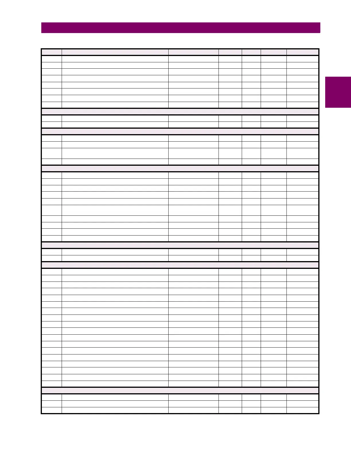
E246 PMU Aggregator 1 PDC Network Control 0 to 1 --- 1 F102 0 (Disabled)
E247 Aggregator 1 Include PMU1 0 to 1 --- 1 F126 0 (No)
E248 Aggregator 1 Include PMU2 0 to 1 --- 1 F126 0 (No)
E249 Aggregator 1 Include PMU3 0 to 1 --- 1 F126 0 (No)
E24A Aggregator 1 Include PMU4 0 to 1 --- 1 F126 0 (No)
E24B PMU Aggregator 1 ASDUS 1 to 4 --- 1 F001 1
E24C PMU Aggregator 1 Port 1 to 3 --- 1 F001 1
E24D PMU Aggregator 1 Reserved (3 items) 0 to 1 --- 1 F001 0
Phasor Measurement Unit Recording Command (Read/Write Command)
E4D4 PMU 1 Recording Clear Command 0 to 1 --- 1 F126 0 (No)
E4D5 PMU 1 Recording Force Trigger 0 to 1 --- 1 F126 0 (No)
Phasor Measurement Unit Recording (Read/Write Setting)
E4DC PMU 1 Record Function 0 to 1 --- 1 F102 0 (Disabled)
E4DD PMU 1 No of Timed Records 2 to 128 --- 1 F001 10
E4DE PMU 1 Trigger Mode 0 to 1 --- 1 F542 0 (Auto
Overwrite)
E4DF PMU 1 Timed Trigger Position 1 to 50 % 1 F001 10
Phasor Measurement Unit Aggregator Control Block (Read/Write Setting)
E650 PMU Aggregator 1 Control Block SvEna 0 to 4294967295 --- 1 F300 0
E652 PMU Aggregator 1 Control Block Client Control 0 to 4294967295 --- 1 F300 0
E654 PMU Aggregator 1 CB SvEna Default 0 to 4294967295 --- 1 F300 0
E656 PMU Aggregator 1 Control Block ConfRev 1 to 4294967295 --- 1 F003 1
E658 PMU Aggregator 1 Control Block Priority 0 to 7 --- 1 F001 4
E659 PMU Aggregator 1 Control Block IPClass 0 to 1 --- 1 F563 1 (Expedited
Forwarding)
E65A PMU Aggregator 1 Control Block VID 0 to 4095 --- 1 F001 0
E65B PMU Aggregator 1 Control Block APPID 0 to 16383 --- 1 F001 0
E65C PMU Aggregator 1 Control Block IP Address 0 to 4294967295 --- 1 F003 0
E65E PMU Aggregator 1 Control Block Security 0 to 2 --- 1 F001 0
DNP/IEC Points (Read/Write Setting)
E700 DNP/IEC 60870-5-104 Binary Input Points (256 items) 0 to 4294967295 --- 1 F300 0
E900 DNP/IEC 60870-5-104 Analog Input Points (256 items) 0 to 65535 --- 1 F300 0
Synchrocheck (Read/Write Setting) (4 modules)
EC00 Synchrocheck 1 Function 0 to 1 --- 1 F102 0 (Disabled)
EC01 Synchrocheck 1 V1 Source 0 to 5 --- 1 F167 0 (SRC 1)
EC02 Synchrocheck 1 V2 Source 0 to 5 --- 1 F167 1 (SRC 2)
EC03 Synchrocheck 1 Maximum Voltage Difference 0 to 400000 V 1 F060 10000
EC05 Synchrocheck 1 Maximum Angle Difference 0 to 100 degrees 1 F001 30
EC06 Synchrocheck 1 Maximum Frequency Difference 0 to 2 Hz 0.01 F001 100
EC07 Synchrocheck 1 Dead Source Select 0 to 5 --- 1 F176 1 (LV1 and DV2)
EC08 Synchrocheck 1 Dead V1 Maximum Voltage 0 to 1.25 pu 0.01 F001 30
EC09 Synchrocheck 1 Dead V2 Maximum Voltage 0 to 1.25 pu 0.01 F001 30
EC0A Synchrocheck 1 Live V1 Minimum Voltage 0 to 1.25 pu 0.01 F001 70
EC0B Synchrocheck 1 Live V2 Minimum Voltage 0 to 1.25 pu 0.01 F001 70
EC0C Synchrocheck 1 Target 0 to 2 --- 1 F109 0 (Self-reset)
EC0D Synchrocheck 1 Events 0 to 1 --- 1 F102 0 (Disabled)
EC0E Synchrocheck 1 Block 0 to 4294967295 --- 1 F300 0
EC10 Synchrocheck 1 Frequency Hysteresis 0 to 0.1 Hz 0.01 F001 6
EC11 ...Repeated for Synchrocheck 2
EC22 ...Repeated for Synchrocheck 3
EC33 ...Repeated for Synchrocheck 4
Phasor Measurement Unit Frequency Trigger (Read/Write Setting)
ECCC PMU 1 Frequency Trigger Function 0 to 1 --- 1 F102 0 (Disabled)
ECCD PMU 1 Frequency Trigger Low Frequency 20 to 70 Hz 0.01 F001 4900
ECCE PMU 1 Frequency Trigger High Frequency 20 to 70 Hz 0.01 F001 6100
Table B–10: MODBUS MEMORY MAP (Sheet 67 of 68)
ADDR REGISTER NAME RANGE UNITS STEP FORMAT DEFAULT
 Loading...