B-66 L30 Line Current Differential System GE Multilin
B.4 MEMORY MAPPING APPENDIX B
B
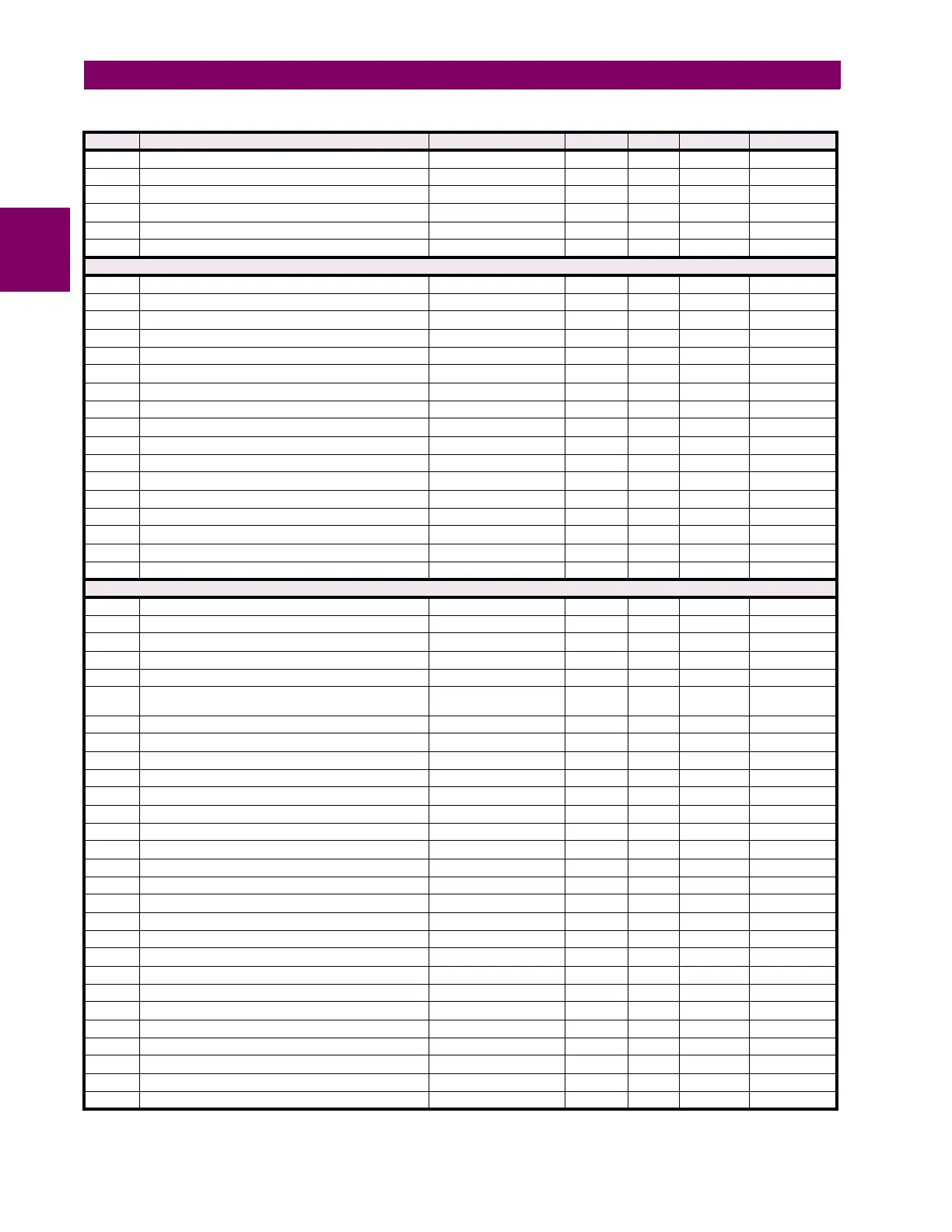
D35A IEC 61850 GGIO2.CF.SPCSO59.ctlModel Value 0 to 2 --- 1 F001 1
D35B IEC 61850 GGIO2.CF.SPCSO60.ctlModel Value 0 to 2 --- 1 F001 1
D35C IEC 61850 GGIO2.CF.SPCSO61.ctlModel Value 0 to 2 --- 1 F001 1
D35D IEC 61850 GGIO2.CF.SPCSO62.ctlModel Value 0 to 2 --- 1 F001 1
D35E IEC 61850 GGIO2.CF.SPCSO63.ctlModel Value 0 to 2 --- 1 F001 1
D35F IEC 61850 GGIO2.CF.SPCSO64.ctlModel Value 0 to 2 --- 1 F001 1
Remote Device Status (Read Only) (16 modules)
D360 Remote Device 1 StNum 0 to 4294967295 --- 1 F003 0
D362 Remote Device 1 SqNum 0 to 4294967295 --- 1 F003 0
D364 ...Repeated for Remote Device 2
D368 ...Repeated for Remote Device 3
D36C ...Repeated for Remote Device 4
D370 ...Repeated for Remote Device 5
D374 ...Repeated for Remote Device 6
D378 ...Repeated for Remote Device 7
D37C ...Repeated for Remote Device 8
D380 ...Repeated for Remote Device 9
D384 ...Repeated for Remote Device 10
D388 ...Repeated for Remote Device 11
D38C ...Repeated for Remote Device 12
D390 ...Repeated for Remote Device 13
D394 ...Repeated for Remote Device 14
D398 ...Repeated for Remote Device 15
D39C ...Repeated for Remote Device 16
Contact Outputs (Read/Write Setting) (64 modules)
D3E0 Contact Output 1 Name --- --- --- F205 “Cont Op 1"
D3E6 Contact Output 1 Operation 0 to 4294967295 --- 1 F300 0
D3E8 Contact Output 1 Seal In 0 to 4294967295 --- 1 F300 0
D3EA Latching Output 1 Reset 0 to 4294967295 --- 1 F300 0
D3EC Contact Output 1 Events 0 to 1 --- 1 F102 1 (Enabled)
D3ED Latching Output 1 Type 0 to 1 --- 1 F090 0 (Operate-
dominant)
D3EE Reserved --- --- --- F001 0
D3EF ...Repeated for Contact Output 2
D3FE ...Repeated for Contact Output 3
D40D ...Repeated for Contact Output 4
D41C ...Repeated for Contact Output 5
D42B ...Repeated for Contact Output 6
D43A ...Repeated for Contact Output 7
D449 ...Repeated for Contact Output 8
D458 ...Repeated for Contact Output 9
D467 ...Repeated for Contact Output 10
D476 ...Repeated for Contact Output 11
D485 ...Repeated for Contact Output 12
D494 ...Repeated for Contact Output 13
D4A3 ...Repeated for Contact Output 14
D4B2 ...Repeated for Contact Output 15
D4C1 ...Repeated for Contact Output 16
D4D0 ...Repeated for Contact Output 17
D4DF ...Repeated for Contact Output 18
D4EE ...Repeated for Contact Output 19
D4FD ...Repeated for Contact Output 20
D50C ...Repeated for Contact Output 21
D51B ...Repeated for Contact Output 22
Table B–10: MODBUS MEMORY MAP (Sheet 58 of 63)
ADDR REGISTER NAME RANGE UNITS STEP FORMAT DEFAULT