Table of Figures
Figure 1: Key to logic diagrams 10
Figure 2: Functional Overview 11
Figure 3: Hardware architecture 30
Figure 4: Coprocessor hardware architecture 31
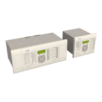
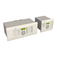
Figure 5: Exploded view of IED 32
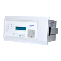
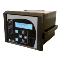
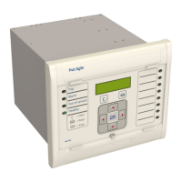
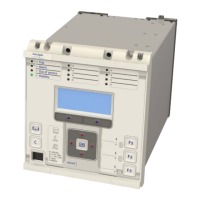
Figure 6: Front panel (60TE) 35
Figure 7: Rear view of populated case 39
Figure 8: Terminal block types 40
Figure 9: Rear connection to terminal block 41
Figure 10: Main processor board 42
Figure 11: Power supply board 43
Figure 12: Power supply assembly 44
Figure 13: Power supply terminals 45
Figure 14: Watchdog contact terminals 46
Figure 15: Rear serial port terminals 47
Figure 16: Input module - 1 transformer board 47
Figure 17: Input module schematic 48
Figure 18: Transformer board 49
Figure 19: Input board 50
Figure 20: Standard output relay board - 8 contacts 51
Figure 21: IRIG-B board 52
Figure 22: Fibre optic board 53
Figure 23: Rear communication board 54
Figure 24: Ethernet board 54
Figure 25: Redundant Ethernet board 56
Figure 26: Fully populated Coprocessor board 58
Figure 27: Software Architecture 64
Figure 28: Frequency Response (indicative only) 71
Figure 29: Navigating the HMI 78
Figure 30: Default display navigation 80
Figure 31: Circuit Breaker Trip Conversion Logic Diagram (Module 63) 87
Figure 32: Sample multi-ended system 100
Figure 33: Current differential discriminative criterion 101
Figure 34: Overall scheme designed for multi-ended differential protection 103
Figure 35: Two-ended transmission line 104
Figure 36: Ping-pong measurement for alignment of current signals 106
Figure 37: Snapshot of available data for processing at each terminal 108
Figure 38: CT saturation technique 109