- 58 -
BIOS Setup
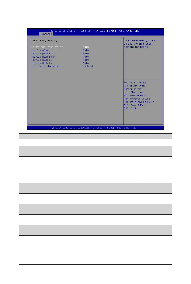
2-2-12-3-2 DRAM Memory Mapping
Parameter Description
DRAM Memory Mapping
Chipselect Interleaving
Interleave memory blocks across the DRAM chip selects for node 0.
Options available: Auto, Disabled. Default setting is Auto.
BankGroupSwap
CongurestheBankGroupSwap.BankGroupSwap(BGS)isanewmemory
mapping option in AGESA that alters how applications get assigned to
physical locations within the memory modules. When this option sets to
Auto, it is null: No help string.
Options available: Auto, Enabled, Disabled. Default setting is Auto.
BankGroupSwapAlt
CongurestheBankGroupSwapAlt.
Options available: Auto, Enabled, Disabled. Default setting is Auto.
Address Hash Bank
Enable/Disable bank address hashing.
Options available: Auto, Enabled, Disabled. Default setting is Auto.
Address Hash CS
Enable/Disable CS address hashing.
Options available: Auto, Enabled, Disabled. Default setting is Auto
Address Hash Rm
Enable/Disable RM address hashing.
Options available: Auto, Enabled, Disabled. Default setting is Auto
SPD Read Optimization
Enable/Disable SPD Read Optimization.
Options available: Auto, Enabled, Disabled. Default setting is Auto
 Loading...