8545-0198-01 Revision 1.9 STX3 Users Manual
9/24/2020 Globalstar, Inc. Confidential and Proprietary Page | 11
Figure 8 Controlled Impedance Calculation
4.2 Effect of Plastic on Radiation
The design of the enclosure must take into consideration the proximity of any material to the antenna. There should be no
conducting material over the antenna. The enclosure must also provide a minimum of 100 mils clearance around the antenna to
minimize the effect of the enclosure on the antenna performance.
The final design should include a measurement of the antenna performance when inside the enclosure. The enclosure may affect
the performance of the antenna by changing the characteristic impedance of the antenna (de-tuning).
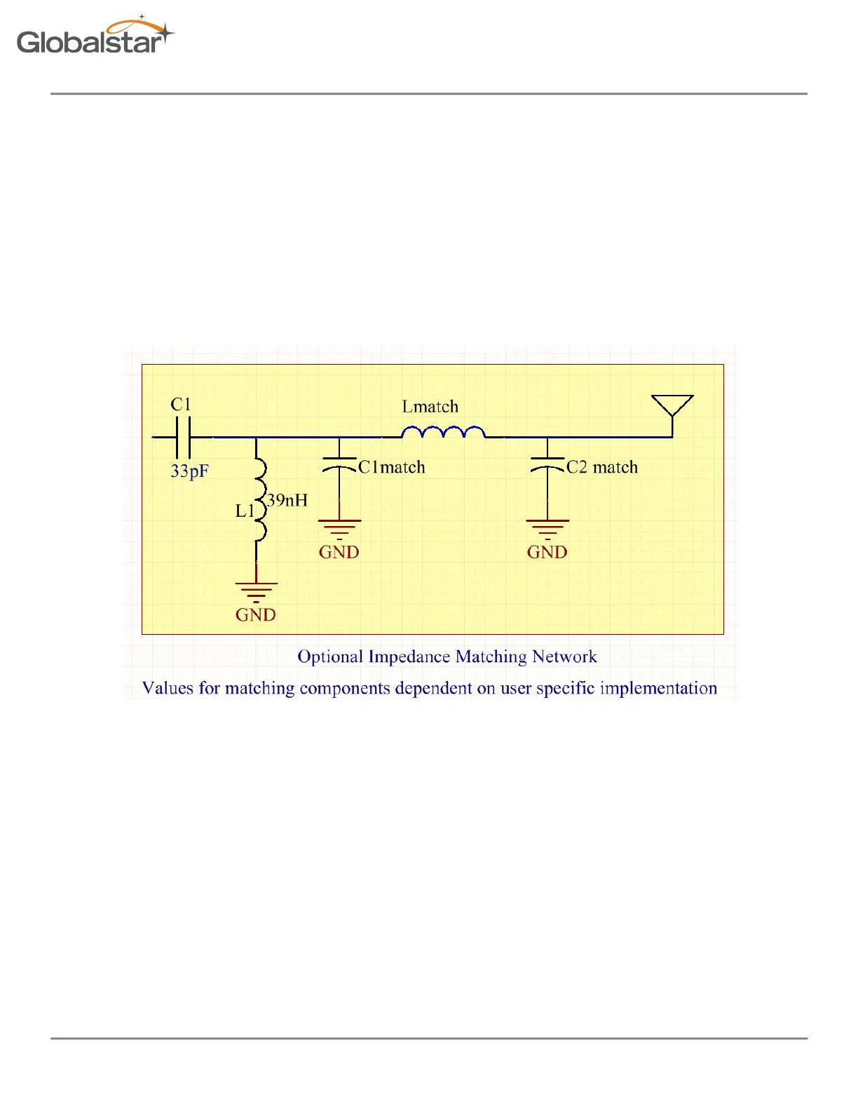
A matching network may be required in the antenna feed to offset the effect of the enclosure and ensure proper performance of the
antenna. Values for matching components are dependent on the user specific implementation.
Figure 9 Antenna Matching Network
The measured return loss should be maintained below -10dB across the operating frequency range of 1610-1620 MHz.
4.3 Power Supply Design
The power supply is sourced by a 3.0V - 5.0V input (VBATT). The digital supply (VDIG) is provided directly from the VBATT supply.
VDIG provides the standby power for the STX3. In standby mode, the STX3 will respond to serial commands via the serial port.
For the high-current active mode, the RF supply (VRF) is provided by a buck/boost switching power supply which can provide the
high current required for transmissions over the satellite network. The open collector output of the STX3 (PWR_EN) is used to turn
on the high-current supply during transmissions. This allows the circuit to maintain a low stand-by sleep current when not actively
transmitting. The VRF power must be stable within 25ms after PWR_EN is activated.
The VBATT supply must be capable of providing up to 475 mA of current during the packet transmissions.