T5CC1
2.2 Pin Names and Functions
The names of the input/output pins and their functions are described below.
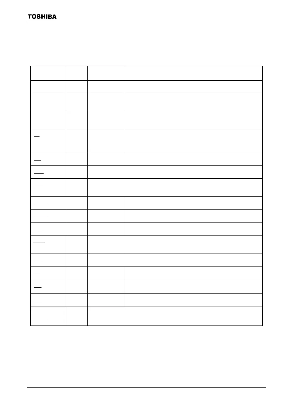
Table 2.2.1 Pin names and functions.
Table 2.2.1 Pin names and functions (1/3)
Pin Name
Number
of Pins
I/O Functions
P00∼P07
AD0
∼AD7
8 I/O
I/O
Port 0: I/O port that allows I/O to be selected at the bit level
Address and data (lower): Bits 0 to 7 of address and data bus
P10∼P17
AD8
∼AD15
A8
∼A15
8 I/O
I/O
Output
Port 1: I/O port that allows I/O to be selected at the bit level
Address and data (upper): Bits 8 to 15 for address and data bus
Address: Bits 8 to 15 of address bus
P20∼P27
A0
∼A7
A16
∼A23
8 I/O
Output
Output
Port 2: I/O port that allows I/O to be selected at the bit level
Address: Bits 0 to 7 of address bus
Address: Bits 16 to 23 of address bus
P30
RD
1 Output
Output
Port 30: Output port
Read: Strobe signal for reading external memory
This port output RD signal also case of reading internal-area by setting P3
<P30>
= 0 and P3FC <P30F> = 1.
P31
WR
1 Output
Output
Port 31: Output port
Write: Strobe signal for writing data to pins AD0 to AD7
P32
HWR
1 I/O
Output
Port 32: I/O port (with pull-up resistor)
High Write: Strobe signal for writing data to pins AD8 to AD15
P33
WAIT
1 I/O
Input
Port 33: I/O port (with pull-up resistor)
Wait: Pin used to request CPU bus wait
((1+N) WAIT mode)
P34
BUSRQ
1 I/O
Input
Port 34: I/O port (with pull-up resistor)
Bus Request: Signal used to request Bus Release
P35
BUSAK
1 I/O
Output
Port 35: I/O port (with pull-up resistor)
Bus Acknowledge: Signal used to acknowledge Bus Release
P36
W/R
1 I/O
Output
Port 36: I/O port (with pull-up resistor)
Read/Write: 1 represents Read or Dummy cycle; 0 represents Write cycle.
P37
BOOT
1 I/O
Input
Port 36: I/O port (with pull-up resistor)
This pin sets single boot mode.
When released reset, Single boot mode is started at P37
=Low level.
P40
CS0
1 I/O
Output
Port 40: I/O port (with pull-up resistor)
Chip Select 0: Outputs 0 when address is within specified address area
P41
CS1
1 I/O
Output
Port 41: I/O port (with pull-up resistor)
Chip Select 1: Outputs 0 if address is within specified address area
P42
CS2
1 I/O
Output
Port 42: I/O port (with pull-up resistor)
Chip Select 2: Outputs 0 if address is within specified address area
P43
CS3
1 I/O
Output
Port 43: I/O port (with pull-up resistor)
Chip Select 3: Outputs 0 if address is within specified address area
P50∼P57
AN0
∼AN7
ADTRG
8 Input
Input
Input
Port 5: Pin used to input port
Analog input: Pin used to input to AD converter
AD Trigger: Signal used to request start of AD converter (Shared with53 pin)
T5CC1 2006-03-03
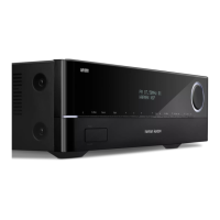
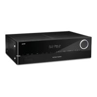
AVR 139-141-142/230 Service Manual
 Loading...