HY57V161610E
Rev. 0.2 / Aug. 2003 2
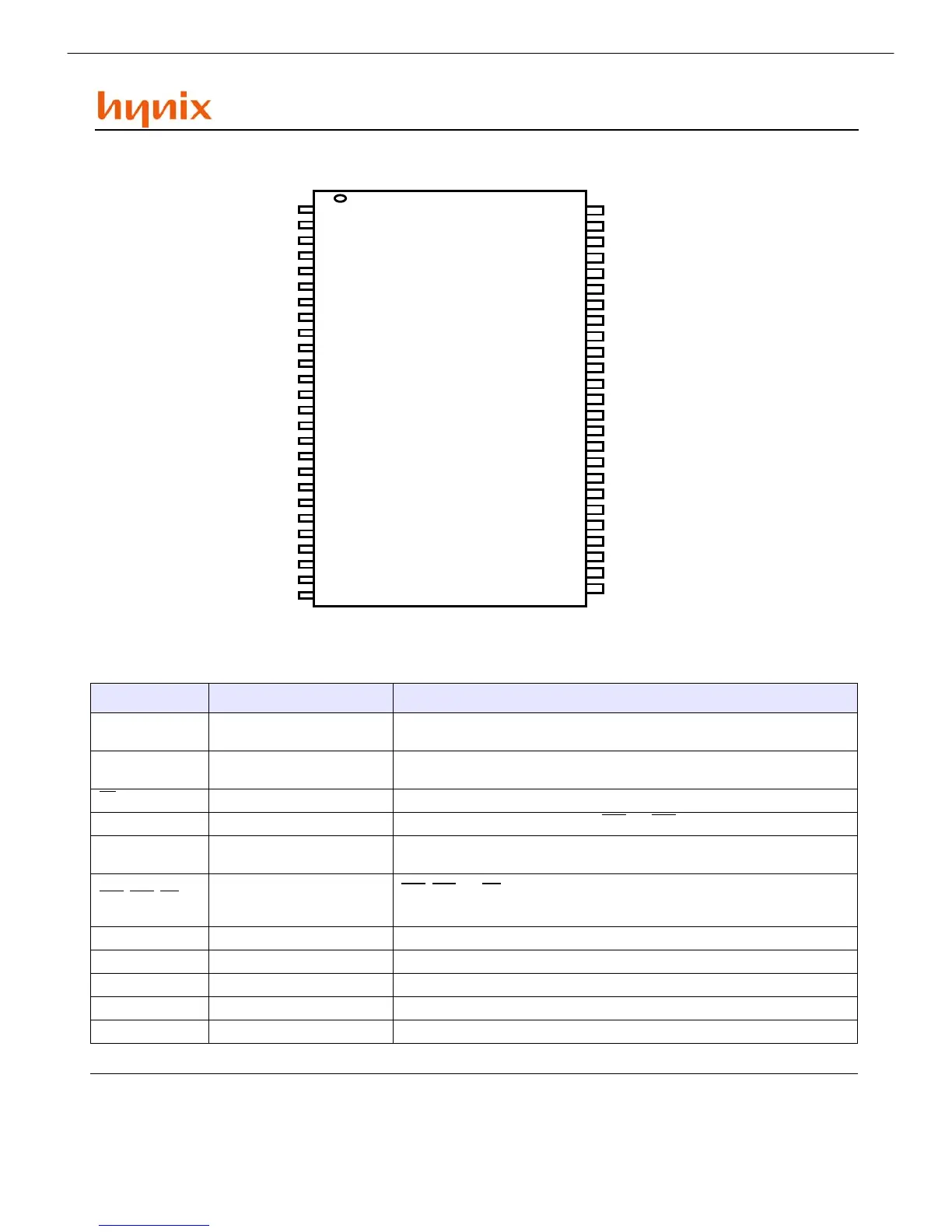
PIN CONFIGURATION
V
SS
DQ15
DQ14
VSSQ
DQ13
DQ12
VDDQ
DQ11
DQ10
VSSQ
DQ9
DQ8
VDDQ
NC
UDQM
CLK
CKE
NC
A9
A8
A7
A6
A5
A4
VSS
1
2
3
4
5
6
7
8
9
10
11
12
13
14
15
16
17
18
19
20
21
22
23
24
25
50
49
48
47
46
45
44
43
42
41
40
39
38
37
36
35
34
33
32
31
30
29
28
V
DD
DQ0
DQ1
V
SSQ
DQ2
DQ3
V
DDQ
DQ4
DQ5
V
SSQ
DQ6
VDDQ
/WE
/CAS
/RAS
/CS
A11
A10
A0
A1
A2
A3
V
DD
50pin TSOP II
400mil x 825mil
0.8mm pin pitch
27
26
DQ7
LDQM
V
SS
DQ15
DQ14
VSSQ
DQ13
DQ12
VDDQ
DQ11
DQ10
VSSQ
DQ9
DQ8
VDDQ
NC
UDQM
CLK
CKE
NC
A9
A8
A7
A6
A5
A4
VSS
1
2
3
4
5
6
7
8
9
10
11
12
13
14
15
16
17
18
19
20
21
22
23
24
25
50
49
48
47
46
45
44
43
42
41
40
39
38
37
36
35
34
33
32
31
30
29
28
V
DD
DQ0
DQ1
V
SSQ
DQ2
DQ3
V
DDQ
DQ4
DQ5
V
SSQ
DQ6
VDDQ
/WE
/CAS
/RAS
/CS
A11
A10
A0
A1
A2
A3
V
DD
50pin TSOP II
400mil x 825mil
0.8mm pin pitch
27
26
DQ7
LDQM
PIN DESCRIPTION
PIN PIN NAME DESCRIPTION
CLK Clock
The system clock input. All other inputs are referenced to the SDRAM on the rising
edge of CLK.
CKE Clock Enable
Controls internal clock signal and when deactivated, the SDRAM will be one of the
states among power down, suspend or self refresh.
CS
Chip Select Command input enable or mask except CLK, CKE and DQM
BA Bank Address Select either one of banks during both RAS
and CAS activity.
A0 ~ A10 Address
Row Address : RA0 ~ RA10, Column Address : CA0 ~ CA7
Auto-precharge flag : A10
RAS
, CAS, WE
Row Address Strobe,
Column Address Strobe, Write
Enable
RAS
, CAS and WE define the operation.
Refer function truth table for details
LDQM, UDQM Data Input/Output Mask DQM control output buffer in read mode and mask input data in write mode
DQ0 ~ DQ15 Data Input/Output Multiplexed data input / output pin
V
DD/VSS Power Supply/Ground Power supply for internal circuit and input buffer
V
DDQ/VSSQ Data Output Power/Ground Power supply for DQ
NC No Connection No connection
 Loading...