EasyManua.ls Logo

Harman Kardon AVR130 Service Manual

Harman Kardon AVR130
114 pages
To Next Page IconTo Next Page
Page #1 background imageLoading...
Page #1 background image
harman/kardon
AVR130
5 X 45W 5.1 CHANNEL A/V RECEIVER
SERVICE MANUAL
CONTENTS
ESD WARNING……………………………….2
LEAKAGE TESTING……………….…..…....3
BASIC SPECIFICATIONS…………………..4
FRONT PANEL CONTROLS………..…..…..5
REAR PANEL CONNECTIONS………….…7
REMOTE CONTROL FUNCTIONS.…….….9
TROUBLESHOOTING GUIDE…...……..…13
PROCESSOR RESET……………….….…..13
DISASSEMBLY……………….……...………14
BULLETIN HK2003-10……………….….…..15
UNIT EXPLODED VIEW……………….…..17
BLOCK DIAGRAM…….........................….18
AMP BIAS ADJUSTMENT………………...19
PCB DRAWINGS…………………………..20
ELECTRICAL PARTS LIST……………….26
SEMICONDUCTOR PINOUTS……………55
SCHEMATICS………………………………97
WIRING DIAGRAM…………………….…..113
PACKAGING…………………………….….114
harman/kardon, Inc.
250 Crossways Park Dr.
Woodbury, New York 11797 Rev1 11/2004
Question and Answer IconNeed help?

Do you have a question about the Harman Kardon AVR130 and is the answer not in the manual?

Harman Kardon AVR130 Specifications

General IconGeneral
Signal-to-Noise Ratio100dB
Total Harmonic Distortion0.07%
Output Impedance8 Ohms
Input Sensitivity200mV
Input Impedance47k Ohms
Tuner Presets30
Frequency Response10Hz to 100kHz
Inputs1 x Coaxial Digital, 1 x Optical Digital
Outputs1 x Audio
Dimensions440 x 150 x 382 mm

Summary

Electrostatic Discharge Precautions

Safety Precautions

Leakage Current Check

Procedure to measure leakage current to ensure safety.

Technical Specifications

Audio Specifications

Details on stereo and surround sound audio performance.

Tuner Specifications

FM and AM tuner frequency range, sensitivity, and distortion.

Video Specifications

Video signal format, frequency response, and input/output levels.

General Specifications

Power requirements, dimensions, and weight of the unit.

Front Panel Controls

Rear Panel Connections

Input and Output Connectors

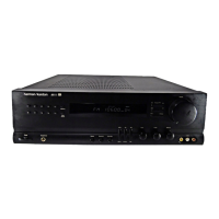
Jacks for audio, video, digital signals, and speaker outputs.

Power, Antenna, and Accessory Ports

AC power input, antenna terminals, and accessory outlets.

Remote Control Functions

Power, Input, and Tuner Controls

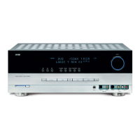
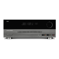
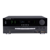
Buttons for unit power, input selection, tuner operations, and display dimming.

Audio Mode and DSP Selection

Buttons for selecting surround modes, DSP, and stereo playback options.

Setup, Navigation, and Special Functions

Buttons for system setup, navigation, macros, and other remote functions.

Troubleshooting Guide

Unit Malfunctions and Solutions

Common unit issues like no power, no sound, or remote unresponsiveness.

Processor Reset Procedure

Steps to reset the unit's system memory and configuration data.

Disassembly Procedures

Top Cover and Front Panel Removal

Instructions for removing the top cover and front panel assembly.

Internal Component Layout

Diagram showing the location of major internal components.

Service Bulletin H/K2003-10

Volume Level Control Issue

Addresses erratic volume control and display tracking issues.

Volume Encoder Replacement Procedure

Step-by-step instructions for replacing the volume encoder.

Exploded View

Schematics and Diagrams

AVR130 Block Diagram

Overall block diagram illustrating the unit's functional layout.

Amplifier Bias Adjustment

Bias Adjustment Procedure

Details on measurement conditions, standard values, and adjustment points.

Electrical Parts List

Front Panel and Input/Output Components

Components for front panel, input/output boards, and miscellaneous connectors.

Main, Video, and Power Supply Components

Components for main board, video board, bias circuitry, and power supply.

IC Block Diagrams and Pin Functions

Transistor and Regulator IC Diagrams

Block diagrams for various transistor and regulator ICs.

TC9162AF Pin Functions

Detailed pin assignment and function description for TC9162AF.

System Block Diagram

Unit Dimensions and Pin Connections

Outer Dimensions Diagram

Diagram showing the physical dimensions and layout of the unit.

Pin Connection Diagram

Diagram illustrating pin assignments for the main IC.

IC Data and Pin Information

LC74763/74763M Pin Assignment

Pinout diagram and assignment for the LC74763/74763M IC.

Serial Data Input Timing

Timing diagram illustrating serial data input sequences.

IC Pin Functions

LC74763M Pin Functions

Detailed description of each pin's function for the LC74763M IC.

System Block Diagram

IC Pin Assignment

AK4114VQ Pin Assignment

Pinout diagram and assignment for the AK4114VQ IC.

IC Block Diagrams

Serial and Parallel Control Mode Diagrams

Block diagrams for serial and parallel control modes.

IC Pin Descriptions

S3C84BB/F84BB Pin Descriptions

Detailed pin assignments and functions for the S3C84BB/F84BB IC.

IC Pin Descriptions (Continued)

S3C84BB/F84BB Pin Descriptions (Continued)

Continued pin descriptions for S3C84BB/F84BB IC.

IC Block Diagram

NJM2296M Block Diagram

Block diagram for the NJM2296M operational amplifier.

IC Pin Configuration and Description

R-6VT Pin Details

Pinout and pin descriptions for R-6VT.

IC Pin Configuration and Description

R-5VL Pin Details

Pinout and pin descriptions for R-5VL.

IC Block Diagrams

TC9164AF Block Diagram

Block diagram for TC9164AF Hex Inverter.

TC9163AF Block Diagram

Block diagram for TC9163AF Hex Inverter.

IC Description and Block Diagram

NJM2581 Description and Block Diagram

General description and block diagram for NJM2581 video amplifier.

IC Equivalent Circuit

NJM2581 Equivalent Circuit

Equivalent circuit diagrams for NJM2581 pins.

IC Block Diagram and Pin Assignment

S3C84BB/F84BB Block Diagram

Block diagram for the S3C84BB/F84BB microcontroller.

IC Pin Assignment

S3C84BB/F84BB Pin Assignment

Pinout diagram for the S3C84BB/F84BB microcontroller.

IC Pin Descriptions

S3C84BB/F84BB Pin Descriptions

Detailed pin descriptions for S3C84BB/F84BB ports.

IC Pin Descriptions (Continued)

S3C84BB/F84BB Pin Descriptions (Continued)

Continued pin descriptions for S3C84BB/F84BB ports.

IC Pin Descriptions (Continued)

S3C84BB/F84BB Pin Descriptions (Continued)

Further pin descriptions for S3C84BB/F84BB ports.

IC Pin Assignment

MB90482 Pin Assignment

Pinout diagram for the MB90482 microcontroller.

IC Pin Descriptions

MB90482 Pin Descriptions

Detailed pin descriptions for MB90482 microcontroller.

IC Pin Descriptions (Continued)

MB90482 Pin Descriptions (Continued)

Continued pin descriptions for MB90482 microcontroller.

IC Pin Descriptions (Continued)

MB90482 Pin Descriptions (Continued)

Further pin descriptions for MB90482 microcontroller.

IC Pin Descriptions (Continued)

MB90482 Pin Descriptions (Continued)

Final pin descriptions for MB90482 microcontroller.

IC Logic Symbol and Truth Table

74HCU04AFN Logic Symbol and Truth Table

Logic symbol and truth table for the 74HCU04AFN hex inverter.

IC Description and Pin Configuration

NJM2068 Description and Pin Configuration

General description and pin configuration for NJM2068 operational amplifier.

IC Pin Assignment and Block Diagram

CS493263 Pin Assignment

Pinout diagram for the CS493263 audio processor.

CS493263 Block Diagram

Block diagram for the CS493263 audio processor.

Audio DSP Pin Functions

CS493263 Pin Functions

Detailed pin functions for the CS493263 audio DSP.

DAC Description and Features

AK4358 24bit DAC Description

General description and features of the AK4358 eight-channel DAC.

DAC Pin Layout

AK4358VQ Pin Layout

Pin layout diagram for the AK4358VQ DAC.

DAC Pin/Function

AK4358 Pin/Function (TBD)

Pin and function definitions for the AK4358 DAC.

ADC Description and Features

AK5381 ADC Description and Features

General description and features of the AK5381 stereo A/D converter.

ADC Compatibility and Layout

AK5381 Compatibility with AK5380

Comparison of AK5381 features with AK5380.

AK5381 Pin Layout

Pin layout diagram for the AK5381 ADC.

ADC Pin/Function

AK5381 Pin/Function

Pin and function definitions for the AK5381 ADC.

IC Function Diagram and Pin Description

HCF4053B Function Diagram

Functional diagram for the HCF4053B analog multiplexer.

HCF4053B Pin Description

Pin description and truth table for HCF4053B.

IC Block Diagram

TC9459F Block Diagram

Block diagram for the TC9459F volume control IC.

IC Pin Description

TC9459F Pin Description

Pin name, function, and remarks for TC9459F.

Main Board 1 (Amplifier) Schematic

Main Board 1 (Amplifier) Schematic (Continued)

Main Board 1 (Amplifier) Schematic (Continued)

Video Board Schematic

Video Board Schematic (Continued)

Video Board Schematic (Continued)

Front Board Schematic

Front Board Schematic (Continued)

Front Board Schematic (Continued)

Main Board 2 (Bias & Regulator) Schematic

Input Board 1 (Analog) Schematic

Input Board 1 (Analog) Schematic (Continued)

Input Board 1 (Analog) Schematic (Continued)

Input Board 2 (Digital) Schematic

Input Board 2 (Digital) Schematic (Continued)

Input Board 2 (Digital) Schematic (Continued)

Wiring Diagram

Packaging and Accessories

Instruction Manual and Accessories

Illustrations and list of included accessories and manuals.

Package Drawing

Diagram showing the product packaging and contents.

Related product manuals