ASAHI KASEI [AK4384]
MS0176-E-00 2002/09
- 2 -
n
Ordering Guide
AK4384VT -40
∼
+85
°
C 16pin TSSOP (0.65mm pitch)
AKD4384 Evaluation Board for AK4384
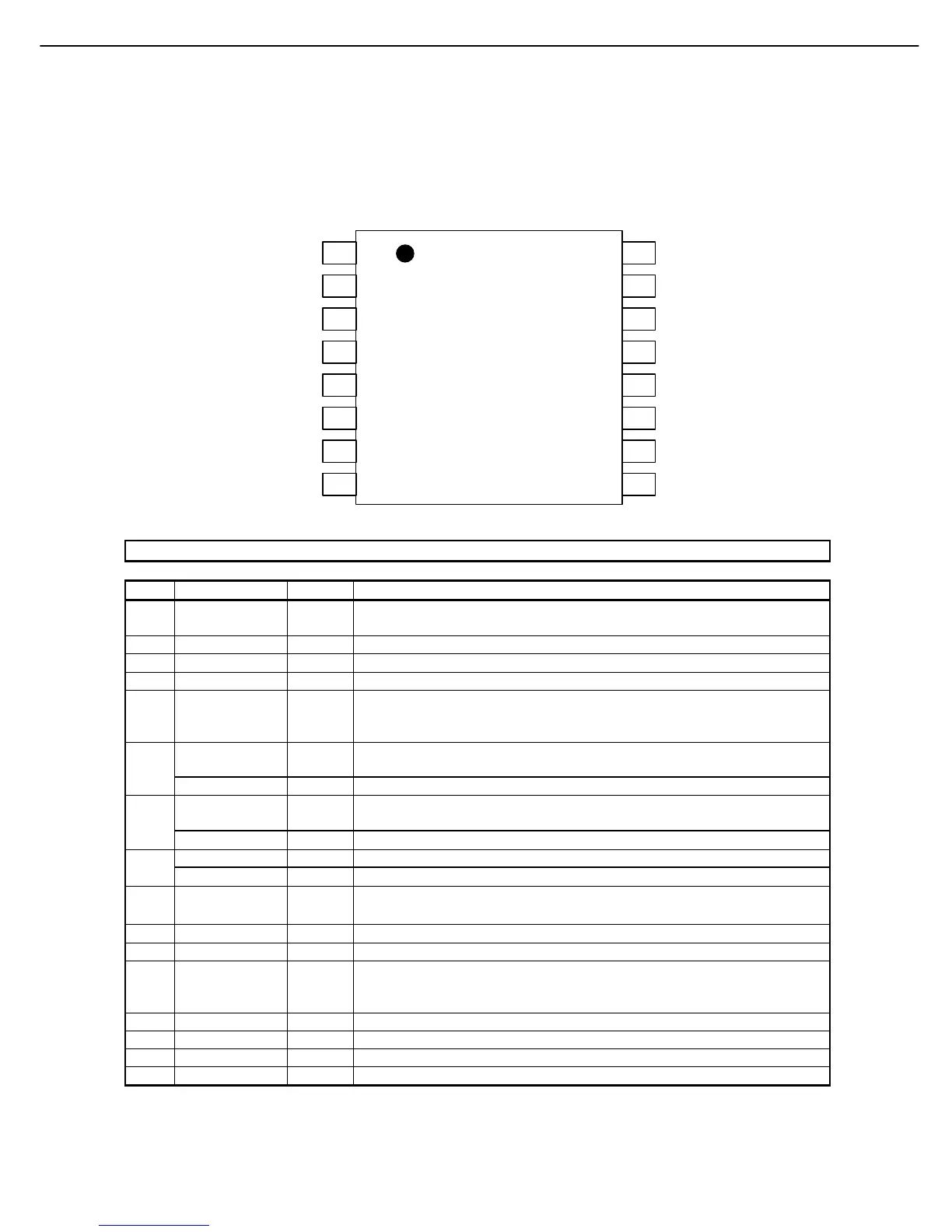
n Pin Layout
1
LRCK
BICK
SMUTE/CSN
ACKS/CCLK
DIF0/CDTI
Top
View
2
3
4
5
6
7
8
DZFL
DZFR
VSS
VDD
AOUTL
AOUTR
P/S
16
15
14
13
12
11
10
9
PDN
PIN/FUNCTION
No. Pin Name I/O Function
1 MCLK I Master Clock Input Pin
An external TTL clock should be input on this pin.
2 BICK I Audio Serial Data Clock Pin
3 SDTI I Audio Serial Data Input Pin
4 LRCK I L/R Clock Pin
5 PDN I Power-Down Mode Pin
When at “L”, the AK4384 is in the power-down mode and is held in reset. The
AK4384 should always be reset upon power-up.
SMUTE I Soft Mute Pin in parallel mode
“H”: Enable, “L”: Disable
6
CSN I Chip Select Pin in serial mode
ACKS I Auto Setting Mode Pin in parallel mode
“L”: Manual Setting Mode, “H”: Auto Setting Mode
7
CCLK I Control Data Clock Pin in serial mode
DIF0 I Audio Data Interface Format Pin in parallel mode 8
CDTI I Control Data Input Pin in serial mode
9 P/S I
Parallel/Serial Select Pin (Internal pull-up pin)
“L”: Serial control mode, “H”: Parallel control mode
10 AOUTR O Rch Analog Output Pin
11 AOUTL O Lch Analog Output Pin
12 VCOM O Common Voltage Pin, VDD/2
Normally connected to VSS with a 0.1µF ceramic capacitor in parallel with a
10µF electrolytic cap.
13 VSS - Ground Pin
14 VDD - Power Supply Pin
15 DZFR O Rch Data Zero Input Detect Pin
16 DZFL O Lch Data Zero Input Detect Pin
Note: All input pins except pull-up pin should not be left floating.
AVR147 harman/kardon
 Loading...