MB90482
(Continued)
*1 : LQFP : FPT-100P-M05
*2 : QFP : FPT-100P-M06
*3 : The circuit type of MB90V480 is E (CMOS/H).
*4 : The circuit type of MB90V480 is G (CMOS/H).
*5 : The circuit type of MB90V480 is I (NMOS/H)
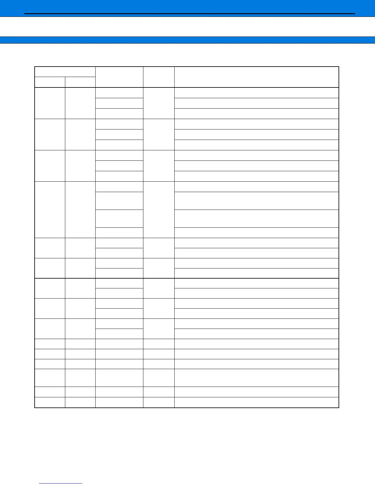
Pin No.
Pin name
Circuit
type
Function
LQFP*
1
QFP*
2
56 58
P90
E
(CMOS/H)
This is a general purpose I/O port.
SIN1 Simple serial I/O data input pin.
CS0 Chip select 0.
57 59
P91
D
(CMOS)
This is a general purpose I/O port.
SOT1 Simple serial I/O data output pin.
CS1 Chip select 1.
58 60
P92
E
(CMOS/H)
This is a general purpose I/O port.
SCK1 Simple serial I/O data input/output pin.
CS2 Chip select 2.
59 61
P93
E
(CMOS/H)
This is a general purpose I/O port.
FRCK
When the free run timer is in use, this pin functions as the
external clock input pin.
ADTG
When the A/D converter is in use, this pin functions as the
external trigger input pin.
CS3 Chip select 3.
60 62
P94
D
(CMOS)
This is a general purpose I/O port.
PPG4 PPG timer output pin.
61 63
P95
D
(CMOS)
This is a general purpose I/O port.
PPG5 PPG timer output pin.
62 64
P96
E
(CMOS/H)
This is a general purpose I/O port.
IN0 Input capture channel 0 trigger input pin.
63 65
P97
E
(CMOS/H)
This is a general purpose I/O port.
IN1 Input capture channel 1 trigger input pin.
64 to 67 66 to 69
PA0 to PA3
D
(CMOS)
These are general purpose I/O ports.
OUT0 to OUT3 Output compare event output pins.
33 35 AV
CC A/D converter power supply pin.
34 36 AVRH A/D converter external reference voltage supply pin.
35 37 AV
SS A/D converter power supply pin.
47 to 49 49 to 51 MD0 to MD2
J
(CMOS/H)
Operating mode selection input pins.
21, 82 23, 84 V
CC 3.3 V ± 0.3 V power supply pins (VCC3) .
9, 40, 79 11, 42, 81 V
SS Power supply input pins (GND) .
AVR330 harman/kardon
 Loading...