1/11September 2001
■ 5V TOLERANT INPUTS
■ HIGH SPEED :
f
MAX
= 150 MHz (MAX.) at V
CC
=3V
■ POWER DOWN PROTECTION ON INPUTS
AND OUTPUTS
■ SYMMETRICAL OUTPUT IMPEDANCE:
|I
OH
|=I
OL
= 24mA (MIN) at V
CC
=3V
■ PCI BUS LEVELS GUARANTEED AT 24 mA
■ BALANCED PROPAGATION DELAYS:
t
PLH
≅ t
PHL
■ OPERATING VOLTAGE RANGE:
V
CC
(OPR) = 2.0V to 3.6V (1.5V Data
Retention)
■ PIN AND FUNCTION COMPATIBLE WITH
74 SERIES 74
■ LATCH-UP PERFORMANCE EXCEEDS
500mA (JESD 17)
■ ESD PERFORMANCE:
HBM > 2000V (MIL STD 883 method 3015);
MM > 200V
DESCRIPTION
The 74LCX74 is a low voltage CMOS DUAL
D-TYPE FLIP FLOP WITH PRESET AND CLEAR
NON INVERTING fabricated with sub-micron
silicon gate and double-layer metal wiring C
2
MOS
technology. It is ideal for low power and high
speed 3.3V applications; it can be interfaced to 5V
signal environment for inputs.
A signal on the D INPUT is transferred to the Q
OUTPUT during the positive going transition of the
clock pulse.
CLR and PR are independent of the clock and
accomplished by a low setting on the appropriate
input.
It has same speed performance at 3.3V than 5V
AC/ACT family, combined with a lower power
consumption.
All inputs and outputs are equipped with
protection circuits against static discharge, giving
them 2KV ESD immunity and transient excess
voltage.
74LCX74
LOW VOLTAGE CMOS DUAL D-TYPE FLIP FLOP
WITH 5V TOLERANT INPUTS
PIN CONNECTION AND IEC LOGIC SYMBOLS
ORDER CODES
PACKAGE TUBE T & R
SOP 74LCX74M 74LCX74MTR
TSSOP 74LCX74TTR
TSSOPSOP
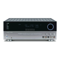
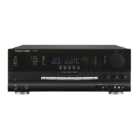
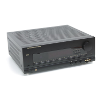
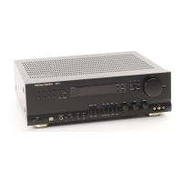
AVR347 harman/kardon
 Loading...