EasyManua.ls Logo

Hi-Link HLK-LD2410S - Hardware Description; Hardware LD2410 S

Hi-Link HLK-LD2410S
33 pages
Print Icon
To Next Page IconTo Next Page
To Previous Page IconTo Previous Page
Loading...
User manual
Page 32 pages in total
5
HLK-LD2410S
Shenzhen Hi-Link Electronic
Co.,Ltd
3. Hardware description
3.1. Hardware LD2410S
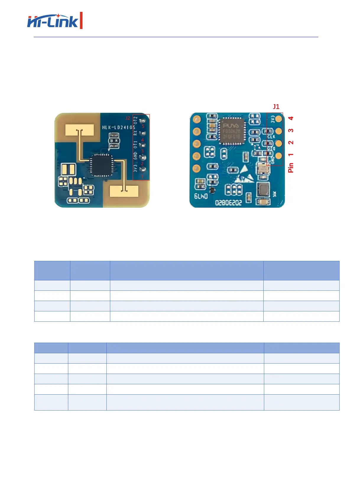
Figure 3-1 shows both sides of the hardware LD2410S. The hardware LD2410S reserve five
pin holes (factory supplied pins) called J2 for power supply and communication. J1 is the SWD
interface for burning and debugging MCU programs.
(a)Front
(b)Back
Figure 3-1 Front and rear of the hardware LD2410S
For details about the pins of J1 and J2, see Table 3-1 and Table 3-2.
Table 3-1 J1 pin description
J#PIN#
Name
Functio
n
Remark
J
1
Pin
1
GND
Grounding
-
J
1
Pin
2
DIO
SWD
Interface data cable
0~3.3
V
J
1
Pin
3
CLK
SWD
Interface clock line
0~3.3
V
J
1
Pin
4
3V3
Power input
3
.
0
V~
3
.
6
V
,
Typ. 3.3
V
Table 3-2 J2 pin description
J#PIN#
Name
Function
Remark
J
1
Pin
1
3V3
Power input
3
.
0
V~
3
.
6
V
,
Typ. 3.3
V
J
1
Pin
2
GND
Grounding
-
J
1
Pin
3
OT1
UART_TX
0~3
.
3
V
J
1
Pin
4
RX
UART_RX
0~3
.
3
V
J
1
Pin
5
OT2
IO, which is used to report the detection status: the high level
is manned, and the low level is unmanned
0~3
.
3
V

Related product manuals